


News: Suppliers
8 September 2021
X-FAB first foundry to offer high-volume micro-transfer printing after licensing agreement with X-Celeprint
Analog/mixed-signal, micro-electro-mechanical system (MEMS) and specialty semiconductor foundry X-FAB Silicon Foundries SE of Tessenderlo, Belgium is now able to support volume heterogeneous integration via micro-transfer printing (MTP) due to a licensing agreement secured with X-Celeprint Ltd of Cork, Ireland – a subsidiary of Tessenderlo-based XTRION N.V. that uses facilities at Ireland’s Tyndall National Institute and in Research Triangle Park, NC, USA to develop and license patented MTP and related technology. A diverse range of semiconductor technologies can hence be combined, each optimized for particular functional requirements. These will include silicon-on-insulator (SOI), gallium nitride (GaN), gallium arsenide (GaAs) and indium phosphide (InP), as well as MEMS.
X-FAB says that, to become the first foundry to provide MTP-based heterogeneous integration, it has made substantial investments over the last two years. It has also established new optimized workflows and cleanroom protocols that will allow customers to work with the foundry on heterogeneous design projects - benefitting from a low-risk and fully scalable business model that offers migration to volume production.
X-Celeprint’s proprietary massively parallel pick-and-place MTP technology stacks and fans-out ultra-thin dies based on different process nodes, technologies and wafer sizes. This results in the formation of virtually monolithic 3D stacked ICs, which have enhanced performance, greater power efficiency, and take up less space. Furthermore, all this can be achieved at an accelerated rate, significantly shortening time-to-market, it is reckoned.
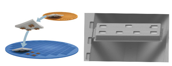
Picture: Micro-transfer-printing-process (left) and X-chip held by nitride tether on source wafer (right).
“By licensing X-Celeprint’s disruptive MTP technology, we are uniquely positioned in our ability to facilitate the incorporation of numerous different semiconductor technologies. X-FAB customers will be able to utilize a technology that no other foundry is offering, and existing X-Celeprint customers may now tap into capacity levels that will easily meet their future demands,” says Volker Herbig, VP of X-FAB’s MEMS business unit. “As a result, we can assist customers looking to implement complete multi-functional subsystems at the wafer level, even when there are high degrees of complexity involved. Signal conditioning, power, RF, MEMS, and CMOS sensors, optoelectronic devices, optical filters, and countless other possibilities will all be covered,” he adds.
“Our agreement with X-FAB represents a major milestone in the commercialization of MTP technology, broadening the number of customers and applications,” reckons X-Celeprint’s CEO Kyle Benkendorfer. “High-volume heterogeneous integration of elements derived from various different source wafers will provide the semiconductor industry with significant new capabilities, including access to higher-density devices with more functionality, fabricated at high yields and lower cost, within shorter timeframes.”


