


News: Optoelectronics
7 April 2022
Microcavity QCL in CW operation at +5C
China’s Institute of Semiconductors claims the first continuous wave (CW) operation of microcavity quantum cascade lasers (QCLs) up to a temperature of 5C at an emission wavelength of 8μm [Qiangqiang Guo et al, ACS Photonics, published online 14 March 2022].
The researchers comment: “The CW operating temperature far exceeds the freezing point and makes it possible to produce portable systems for use outside a laboratory environment.” The team sees prospects for use in photonic integrated circuits, on-chip sensing, and microcavity frequency combs.
The researchers fabricated QCL material from solid-source molecular beam epitaxy on indium phosphide (InP) into high quality factor (Q) notched elliptical whispering gallery mode (WGM) electromagnetic (EM) resonators (Figure 1).
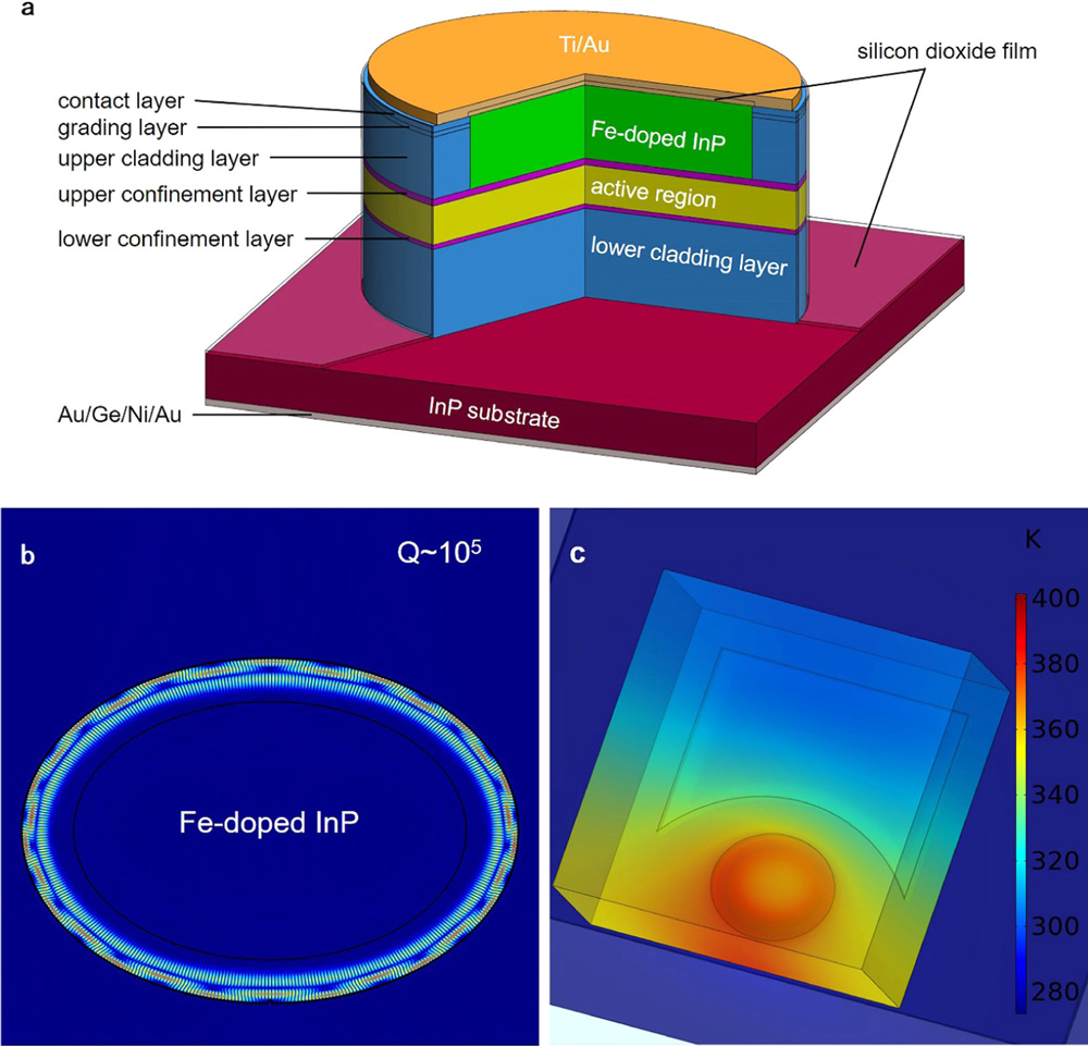
Figure 1: Structure and design of CW microcavity QCL: (a) schematic; (b) calculated mode distribution; (c) simulated three-dimensional temperature profiles.
The 40-stage QCL consisted of layers of indium gallium arsenide (InGaAs) and indium aluminium arsenide. InGaAs was also used for optical confinement.
Since the excited EM modes are concentrated at the periphery of the structure, electrical isolation was introduced in the middle of the structure in the form of semi-insulating InP produced through iron (Fe) doping. The researchers explain: “This reduces the overall injection current, thereby reducing the operating temperature in the active region. Theoretically, this design can eliminate the most unnecessary thermal dissipation, which is the primary limiting factor for CW operation of microcavity QCLs, and simultaneously provide a horizontal channel for the heat dissipation in the active region.”
The Fe-doped InP, produced by wet etching to the upper confinement layer and regrowth, was also close in refractive index to the cladding layers. The sidewalls of the device were optionally passivated with silicon dioxide to suppress leakage current through thermally activated surface states.
The ellipse’s aspect ratio was 1.2 with a semi-minor axis length of 80μm. The wavelength-scale notch – 2.5μm width, 1.6μm depth – was located at the intersection of the minor axis with the boundary. The Fe-doped InP material had a 65μm semi-minor axis.
The electrical isolation scheme was found to more than double the slope efficiency in pulse-mode operation. Passivating the devices with silicon dioxide severely reduced peak output power and increased the threshold current. This was attributed to high optical loss of the passivation at wavelengths above 7μm. The output wavenumber was around 1250/cm, which corresponds to 8μm wavelength.
In CW operation (Figure 2) the side-mode suppression ratio (SMSR) was around 30dB. Devices with electrical isolation and surface passivation were able to operate at temperatures up to +5C. The thermal conductance of this device, 729.8/cm2-K, was much higher than for one without the electrical isolation, 276.9/cm2-K, in line with the simulations carried out to design the lasers.
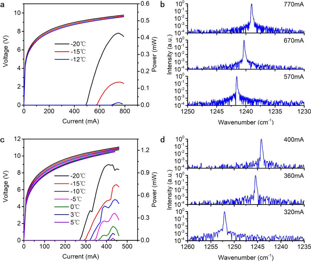
Figure 2: Electrical and optical characteristics of devices with surface passivation in CW operation: (a, c) measured power-current-voltage characteristics versus heatsink temperature (a) without and (c) with electrical isolation; (b, d) CW spectra at -20C versus pumping current corresponding to panels (a) and (c), respectively.
The CW threshold current was reduced by 40% when electrical isolation measures were taken. “This surprising result is due to the reduction of unnecessary heat dissipation power brought about by the electrical isolation, which effectively reduces the operating temperature of the active region,” the team comments.
The wavenumber distance between modes was about 5.42/cm, again close to the simulation result of 5.53/cm. A mode hop was observed in the spectrum of the device with electrical isolation. This creates corresponding kinks in the light output power behavior.
Microcavity quantum cascade lasers InP InGaAs MBE
https://doi.org/10.1021/acsphotonics.1c01437
The author Mike Cooke is a freelance technology journalist who has worked in the semiconductor and advanced technology sectors since 1997.


