


News: Microelectronics
21 April 2022
Speedy, durable, retentive GaN non-volatile memory
Hong Kong University of Science and Technology (HKUST) reports on a gallium nitride (GaN) non-volatile memory (NVM) with good speed, retention and endurance at the same time [Tao Chen et al, IEEE Electron Device Letters, published online 21 March 2022]. In silicon-based NVMs there tends to be a trade-off in these characteristics, creating a manufacturing ‘trilemma’ due to the use of Fowler-Nordheim tunneling across a tunnel oxide (TO) to change the memory state.
The researchers comment: “This work shows that the mainstream GaN-on-Si platform can also accommodate high-performance non-volatile memory devices in addition to the power and radio frequency (RF) devices, to enable highly intelligent electronic systems.”
The device integrated a p-channel field-effect transistor (p-FET) with p-i-n heterojunction diode. The p-FET consisted of aluminium oxide (Al2O3) gate insulator on p-GaN.
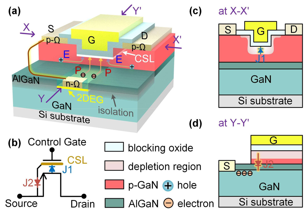
Figure 1: Schematics of GaN-based TO-free BJB memory device: (a) perspective view; (b) circuit symbol; cross-sectional view of (c) cutline X-X’ and (d) cutline Y-Y’.
The charge storage for the memory function occurred at the Al2O3/p-GaN interface. While in normal transistors one doesn’t want interfacial trap states, for the memory function they are specifically created.
A depletion region forms at the Al2O3/p-GaN junction (J1) isolating the charge storage layer (CSL) from the holes in the p-channel of the FET structure.
The memory state can be changed by hole injection from the p-channel or electron injection from the diode (J2), consisting of aluminium gallium nitride between GaN layers (p-GaN/AlGaN/GaN). In particular, a two-dimensional electron gas (2DEG) can form at the AlGaN/GaN junction when the overlying p-channel is fully depleted by an appropriate gate potential or when removed (Figure 2).
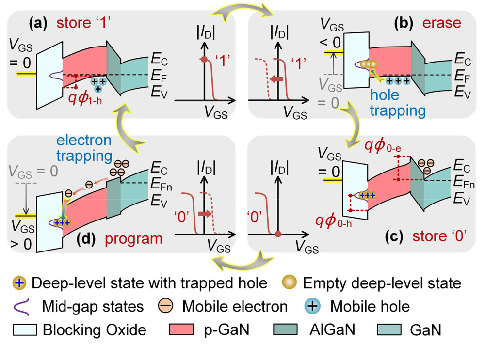
Figure 2: Energy band diagrams and schematic ID-VGS curves of memory in (a) ’1’ state, (b) erase stage, (c) ’0’ state, and (d) program stage. qφ1-h, qφ0-h and qφ0-e are hole diffusion/emission and electron injection barriers in states ’1’ and ’0’, respectively.
Conventionally, hole-based charge storage would have program/erase (P/E) steps based on gate-potential-controlled hole injection/emission, but here electron injection is also possible in a bipolar junction barrier (BJB) structure. The researchers comment: “Such junction-barrier-controlled bipolar charge injections enable fast P/E processes and facilitate to decouple the enhancement of endurance from that of speed and retention.”
The charge state of the CSL was measured through the drain current (ID) at a drain-source potential (VDS) of -0.5V with 0V on the gate (VGS). The low current state was labeled ’0’ and the high ’1’.
The device material was grown on commercial GaN-on-silicon (Si) wafers aimed at enhancement-mode high-electron-mobility transistor manufacturing. The metal-organic chemical vapor depostion growth consisted of 4μm GaN buffer and unintenionally doped n-channel/2DEG, 12nm AlGaN barrier, and 85nm p-GaN.
The NVM structure was fabricated first by patterned plasma etching of the p-GaN to form a 2DEG channel region. Ohmic contacts were made to the 2DEG channel and the source-drain regions of the p-FET. More patterned etching thinned the p-GaN to 35nm in the FET gate area. The surface of the p-GaN at the gate stack interface was treated with oxygen plasma, generating high-density deep-level trap states for the CSL. The traps were covered with 20nm atomic layer deposition (ALD) Al2O3 blocking oxide (BO). The devices were then electrically isolated with fluorine ion implantation. The gate electrode consisted of nickel/gold.
A P/E cycle with 10V/-10V gate potential (VP/E) achieved P/E times of 100μs/100ns. By increasing VP to 20V, the P-time could be reduced to 100ns. The team comments: “The 100ns of P/E time is limited by parasitic effects such as the channel resistance, and thus could be further reduced by device down scaling.”
Retention of the memory states was extrapolated from measurements made at high temperature, 125-200°C, to speed up degradation to a 1V difference in the p-FET threshold potentials for the two memory states. The extrapolated retention came to more than 107s; in fact, retention was estimated at 2.17 years (6.8x10⁷s) at 25°C. The activation energy for the temperature dependence was 0.79eV. The researchers believe this could be increased, giving even longer retention, based on the wider bandgap of GaN relative to silicon.
The endurance under P/E cycling was more than 106 with 20V VP, and 108 for 10V. The lower VP puts the barrier oxide under less electric-field stress, reducing degradation from this source. The degradation results in greater current leakage from the gate into the CSL.
Table 1: Benchmarks of charge-based NVMs. aHSO: silicon-doped HfO2. bExtrapolated value at room temperature.
| Channel material | Gate stack | Program/erase speed | Endurance | Retentionb |
| Si | SiO2/Nitride/SiO2 | 20V/10μs (P)/ -20V/1ms (E) | > 103 | > 108s |
| Si | SiO2/HSO/SiO2a | 17V/300ns (P)/ -16V/300ns (E) | > 105 | > 108s |
| Si | SiO2/Nitride/SiO2 | 22V/1μs (P)/ -16V/10μs (E) | > 107 | > 105s |
| GaN | Al2O3/p-GaN/ AlGaN/GaN | 10V/100μs (P)/ -10V/100ns (E) | > 108 | > 107s |
The usual Si-based NVMs (Table 1 shows typical trade-offs relative to HKUST GaN device) use Fowler-Nordheim tunneling across an insulating oxide to charge the CSL, which needs a high electic field to P/E the state. The HKUST team believes that the electric field across the blocking oxide in its NVM “can be reduced by adopting lower doping concentration in the p-GaN or high-κ dielectric materials without sacrificing the speed and retention performance.”
HKUST GaN Non-volatile memory p-FET ALD
https://doi.org/10.1109/LED.2022.3161010
The author Mike Cooke is a freelance technology journalist who has worked in the semiconductor and advanced technology sectors since 1997.


