


News: LEDs
1 August 2022
Enhancing MOCVD N-polar LEDs
Jilin University and Zhengzhou University in China have reported progress in enhancing the performance of indium gallium nitride (InGaN) light-emitting diodes (LEDs) grown by metal-organic chemical vapor deposition (MOCVD) in the nitrogen- rather than gallium-polar direction [Yang Wang et al, Optics Letters, v47, p3628, 2022]. The researchers hope that their efforts “will facilitate the development of N-polar GaN-based long-wavelength light-emitting devices for application in micro-LED displays.”
The potential advantages of using N-polar III-nitride material include an enhanced incorporation of indium atoms, allowing longer wavelengths to be emitted.
Another benefit in N-polar devices comes from the reversal of the electrical fields arising from the differences in charge polarization of the various III-N bonds in the different heterostructure layers. In Ga-polar material these fields inhibit electron-hole recombination into photons due to the quantum-confined Stark effect (QCSE). The N-polar field reversal of the fields weakens the QCSE.
The polarization field reversal also eliminates the barrier to electron injection into the quantum well (QW) active region, while also increasing the barrier against electron overflow from the QW into the p-type hole injector structure.
Despite these advantages for N-polar devices, the Ga-polar structure still has greater luminous efficiency, which the team hopes will be overtaken in the future by N-polar structures.
Problems for N-polar material include high concentrations of carbon and oxygen impurities, inclusion of zincblende crystal phase material in the target wurtzite crystal structure, and the formation of hexagonal hillocks on the growth surface. The zincblende inclusions tend to result in triangular bulges on the surface of N-polar samples.
The team has previously found some success in reducing carbon/oxygen impurity incorporation by mainly optimizing the V/III precursor supply ratio. The new work mainly focused on reducing zincblende inclusion and hexagonal hillock formation.
The researchers grew N-polar InGaN/GaN double QW (DQW) samples on 2μm-thick N-polar GaN templates on misoriented sapphire.
One strategy deployed by the team, mainly aimed at reducing zincblende inclusion, was to increase the quantum barrier (QB) growth temperature from 845°C to 945°C. The QWs were grown at 745°C. The higher QB growth temperature reduced root-mean-square (RMS) surface roughness to 3.07nm from 11.9nm in the lower-QB-temperature sample, according to atomic force microscopy (AFM) over a 5μmx5μm field.
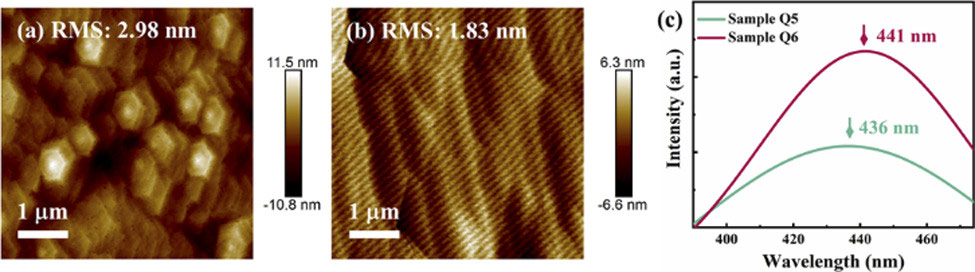
Figure 1. Surface AFM images of N-polar InGaN/GaN DQW samples with 785°C QW, and QBs grown (a) without (Q5) and (b) with (Q6) 1slm hydrogen in the carrier gas. (c) Fitted room-temperature PL spectra.
The researchers comment: “The zincblende-phase inclusions were eliminated due to the increase in the mobility of surface adatoms at elevated temperature.”
Photoluminescence on the samples showed the effect of reduced hillock formation and zincblende inclusion in the form of increased emission and a red-shift in wavelength by 6nm. “The red-shift of the emission wavelength can be attributed to the elimination of zincblende-phase inclusions, which increases the indium incorporation efficiency of the DQWs,” the researchers explain.
Moves to tackle hillock growth included using hydrogen rather than nitrogen as the carrier gas during QB growth. Hydrogen has a high affinity with N-polar surfaces. The team reports: “Owing to the reduction of the diffusion barrier to adatoms on the sample surface achieved by higher hydrogen coverage, the hexagonal hillocks were effectively eliminated, and the surface RMS roughness was further reduced.”
However, a complete switch to hydrogen carrier resulted in triangular step edges on the surface, due to the different speeds of step edge propagation in different directions. The higher adatom incorporation with hydrogen carrier gas aggravates this effect. The RMS roughness with a complete switch to hydrogen was 2.29nm. A sample with a partial replacement of hydrogen in the nitrogen carrier gas at the rate of 1 standard liter per minute (slm) enabled an RMS reduction to 1.51nm.
The addition of hydrogen to the carrier gas during QB growth resulted in still higher emission peaks and a further red-shift of around 9nm. The partial hydrogen addition resulted in a somewhat higher peak than the complete switch to hydrogen.
Increasing the QW growth temperature from 745°C to 785°C shifted the PL peaks from green light with longer than 500nm wavelength to blue at 436nm and 441nm with QBs grown at high temperature without and with 1slm hydrogen in the carrier gas, respectively (Figure 1). The corresponding surface morphologies were 2.98 and 1.83nm RMS. “This demonstrates that the surface morphology of N-polar DQWs has a minor dependence on the QW growth temperature in the temperature range of our experiment,” the team comments.
The researchers also fabricated LEDs from the 436/441nm PL emitting materials (Figure 2). The longer-wavelength material was grown with hydrogen in the carriers gas during QB growth, giving a device labeled LED-A. The reference LED-B was grown without hydrogen in the QB carrier. The LED-A demonstrated much lower series resistance, giving higher current for a given potential bias.
The team comments: “Compared with LED-B, LED-A exhibits significantly improved EL intensity and a longer emission wavelength, which is consistent with the PL measurement results for DQWs before and after optimization.”
The optimized LED-A also showed a ~ 92% higher external quantum efficiency (EQE) peak relative to LED-B. After the peak, the EQE droop at 25A/cm2 injection was 17% and 40% for LED-A and LED-B, respectively. “The significant alleviation of the efficiency droop in LED-A is ascribed to the enhanced carrier confinement brought by the optimized DQWs,” the team explains.
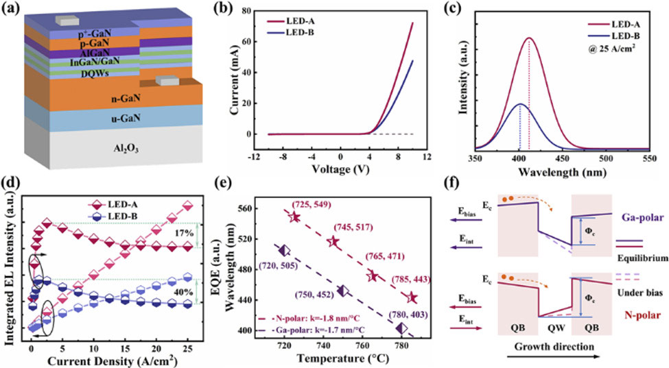
Figure 2. (a) Schematic diagram of the N-polar InGaN/GaN LED. (b) Current–voltage characteristics of LED-A and LED-B (reference sample). (c) Electroluminescence (EL) spectra of LED-A and LED-B under driving current density of 25A/cm2. (d) Integrated EL intensity and relative external quantum efficiency (EQE) of LED-A and LED-B versus driving current density. (e) Emission wavelengths at 10K of N-polar (red) and Ga-polar (purple) DQWs versus QW growth temperature; dotted lines represent linear fit. (f) Conduction-band diagrams of Ga- and N-polar InGaN/GaN QWs at equilibrium and in biased state, showing directions of polarization electric field and applied electric field; Φe represents overflow barrier for electrons from QW towards p-type layers.
The researchers also fabricated N-polar and Ga-polar LEDs with varied QW growth temperatures to tune the indium incorporation, and thus the emission wavelength. The N-polar devices showed around 57nm red-shift in emission wavelength relative to Ga-polar devices with QWs grown at the same temperature.
The team comments: “Theoretical studies indicated that the In atoms in N-polar InGaN are covered by an N-H surface layer, preventing In desorption or replacement by Ga atoms, which is not the case in Ga-polar InGaN.”


