


News: Microelectronics
9 December 2022
High temperature GaN memory and sequential logic
Researchers in the USA and Bangladesh claim the highest operational temperature of 300°C for gallium nitride (GaN) delay flip-flops (DFFs), among other circuits fabricated on a GaN/silicon platform [Mengyang Yuan et al, IEEE Electron Device Letters, v43, p2053, 2022]. Previous DFF demonstrations have only been reported up to 160°C.
The team from Massachusetts Institute of Technology and Bangladesh University of Engineering and Technology also report read-only memory (ROM), static random access memory (SRAM), and data/D-latch components based on n-type field-effect transistors (n-FETs) that operated at 300°C.
The researchers see their achievement as paving the way to robust mixed-signal systems operating at high temperature (HT). They suggest applications in aerospace, automotive, oil and gas exploration. Building on previous achievements in combinational logic, the team has gone on to the next step: the sequential logic needed for storage of state information.
The GaN transistors (Figure 1) for the circuits were fabricated from 150mm GaN/Si wafers with aluminium gallium nitride (AlGaN) barrier and p-type GaN gate layers (p-GaN/AlGaN/GaN/Si), provided by Dr Kai Cheng of Enkris Semiconductor Inc. The p-GaN layer enabled fabrication of the enhancement/E-mode (normally-off at 0V gate/G potential, relative to source/S). The E-mode devices were fabricated using a self-aligned gate-first recipe with tungsten (W) providing a Schottky contact to the p-GaN.
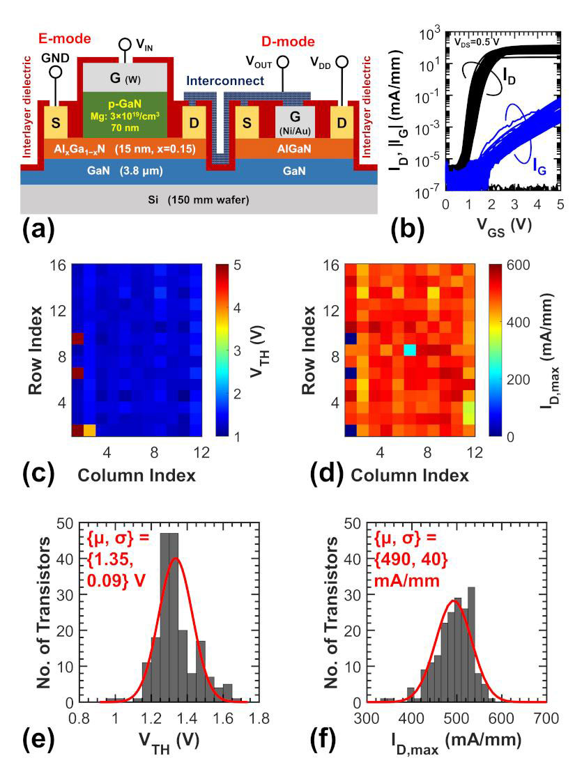
Figure 1: (a) E/D-mode transistors connected as inverter. (b) Transfer characteristics with 0.5V drain bias, (c) distribution and (e) histogram of VTH, and (d) distribution and (f) histogram of ID,max of 192 E-mode transistors across 1.2cmx1.2cm sample at 25°C.
The researchers explain how this enables high-temperature operation: “The E-mode transistor technology of this work was optimized for HT applications through features including, (1) a refractory metal (W) gate, and (2) self-alignment of p-GaN and metal through the gate-first process, which ensures a high metal/p-GaN surface quality and reduces leakage which would become significant problems at HT.”
The back-end-of-line (BEOL) fabrication began with nickel/gold (Ni/Au) for the depletion/D-mode (normally-on) Schottky gate and first layer interconnect between the devices. After adding an insulating silicon dioxide (SiO2) interlayer dielectric, vias were opened for titanium/gold (Ti/Au) contact pads. The Ti/Au was also used for the second layer interconnects.
Both device types featured a 2μm gate length, and 2μm G-S and G-D separations. The 12μm-wide D-mode transistors had a threshold voltage (VTH) around -1V. The more difficult operation of the 36μm-wide E-mode transistors achieved a VTH of +1.35V with a 0.09V standard deviation (σ). The maximum drain current (ID,max) averaged 490mA/mm with 40mA/mm σ. The E-mode transistors served as the drivers for the various circuits fabricated.
The team notes that there is an excess of outliers at the 3σ level: 5% for VTH, 3% for ID,max. This particular measurement setup was not able to be implemented to test performance at HT.
“The circuits which incorporate transistors with significant outlying characteristics would likely not work as expected,” the researchers warn. Mitigating these effects could be achieved through redundancy, but for proof-of-concept the team used circuit designs with large tolerance to transistor performance deviations.
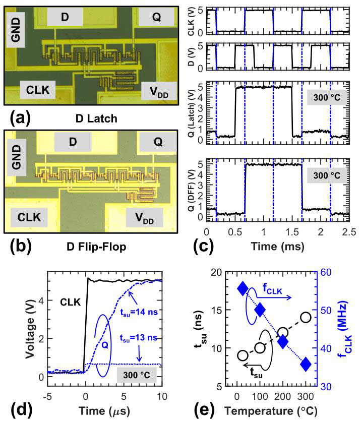
Figure 2: (a) Micrograph of negative multiplexer-based latch. (b) Micrograph of positive DFF. (c) Waveforms of CLK at 1kHz, D at 1.5kHz, and D-latch/DFF outputs (Q). (d) Example determination of tsu, using output waveform of DFF at 300°C. (e) Trend of tsu and estimated fCLK versus temperature.
The operating voltage (VDD) of the circuits was 5V, aiming at balancing speed, noise margin and power consumption. The performance was tested in a probe station with a thermal chuck capable of heating up to 300°C.
The fabricated circuits included a 32bitx10bit NOR-based read-only memory (ROM), a four-transistor static random access memory (4T-SRAM), a 13T multiplexer-based negative data/D latch with input/output buffers, and a 20T positive DFF in a primary-secondary (master-slave) configuration.
The ROM was programmed with its first 10-bit word line set to [1000110001], which was read successfully at 300°C. The SRAM cell also performed stably at 300°C.
The researchers comment on the D-latch and DFF: “A large voltage swing over 4V could still be achieved for both the D latch and the DFF at 300°C due to the matched temperature behavior of the ON-resistance for both the E- and D-mode transistors.”
The clock frequency (fCLK) of the D-latches and DFFs were limited by the set-up time (tsu). This increased from 9ns to 14ns as the temperature increased from 25°C to 300°C, respectively. The maximum clock frequency therefore reduced from 55MHz to 36MHz. “The decrease in performance is mainly due to the decreased ON-current of both E- and D-mode transistors resulting from the reduction of channel mobility at higher temperatures,” the team reports.
The researchers believe improvements can be sought from device scaling, reduced gate leakage, optimized circuit parasitics and chip area, a more thermally robust BEOL process, and monolithically integrated GaN complementary circuit designs.
The author Mike Cooke is a freelance technology journalist who has worked in the semiconductor and advanced technology sectors since 1997.


