


News: Microelectronics
15 December 2022
Vertical GaN junction barrier Schottky diodes
Nagoya University and Toyota Central R&D Labs Inc in Japan claim a record low on-resistance (RON) for vertical gallium nitride (GaN) Schottky barrier diodes (SBDs) of between 0.57mΩ-cm2 and 0.67mΩ-cm2 [Maciej Matys, Appl. Phys. Lett., v121, p203507, 2022]. The breakdown voltages (BVs) of between 660V and 675V, dependent on dimensions, were 84.4% of the value expected for ideal parallel plane structures.
One target for such devices is low-loss power switching applications. Although vertical GaN pn diodes have similar performance in terms of RON and BV, the higher turn-on voltage (VON~3V for pn, compared with 0.74 for Nagoya/Toyota’s SBDs) results in wasted power.
The team comments: “Compared to silicon carbide (SiC) JBS rectifiers, the GaN JBS diodes represent an early stage of development. Thus, the ability to realize high-performance vertical GaN JBS diodes can bring GaN power electronics to the next level.”
The researchers used a junction barrier Schottky (JBS) diode structure (Figure 1). The 10μm drift layer of silicon (Si)-doped n-GaN was grown on freestanding heavily doped substrates by hydride vapor phase epitaxy. The threading dislocation density was of order 106/cm2. The thickness of the drift layer was designed to exceed the 5μm limit for avoiding punch-through at the effective donor concentration (Nd) of 2.5x10¹⁶/cm3.
![Figure 1: (a) Schematic cross section of JBS diode, (b) secondary-ion mass spectroscopy (SIMS) depth profile of [Mg] together with simulated [Mg] depth-profile, (c) optical image of fabricated JBS diode, (d) scanning capacitance microscopy (SCM) image of JBS A, and (e) linear profile of dC/dV obtained along line 1 from SCM image.](22122_nagoya_f1.jpg)
Figure 1: (a) Schematic cross section of JBS diode, (b) secondary-ion mass spectroscopy (SIMS) depth profile of [Mg] together with simulated [Mg] depth-profile, (c) optical image of fabricated JBS diode, (d) scanning capacitance microscopy (SCM) image of JBS A, and (e) linear profile of dC/dV obtained along line 1 from SCM image.
The p-type barrier layer was achieved by magnesium ion implantation to a depth of 2μm, using a silicon dioxide (SiO2) mask. The p-type layer was activated via 30-minute ultra-high-pressure annealing (UHPA), carried out at the Japan Ultra-High Temperature Materials Research Institute. The annealing temperature and pressure were 1300°C and 500MPa, respectively. The box profile of the 2x10¹⁸/cm3 Mg doping was around 0.44μm, deeper than the 0.22μm simulated by Monte Carlo methods due to Mg diffusion during the UHPA.
The channel widths (Ln) of the fabricated JBS diodes A and B were 1.5μm and 1μm, respectively. Mg diffusion reduced these values somewhat by extending the effective width of the p-type regions, according to scanning capacitance microscopy (SCM), although the shrinking of the electrical junction (EJ) in the measurements could also be partly due to AC bias of the SCM tip. Subsequent analysis of the measured RON, compared with a model, suggested this latter factor dominated.
The Schottky electrodes were nickel/gold, while the ohmic bottom contact was titanium/aluminium/nickel/gold. The JBS diodes were square with rounded corners. The active area consisted of periodic n- and p-type regions: 17 for JBS A, and 20 for JBS B.
VON was 0.74V and the ideality around 2. The minimum RON for the devices occurred in the range 1.5–1.6V. An SBD fabricated by the team had an RON of 0.51mΩ-cm2. The forward current of the JBS diodes at 5V was more than 5.5kA/cm2 (0.5A). Above 3V the RON of JBS B reduced to the level of the SBD, suggesting that some current flowed through the p-type regions since the turn-on voltage for vertical pn junctions is around 3V. “The reason for this issue is rather not clear at this moment,” the team adds.
On the basis of the high breakdown voltage, the researchers estimate that the maximum electric field reached 2.47MV/cm, consistent with previous reports of similarly doped n-GaN. The leakage at reverse biases less than 120V was 3-4 orders of magnitude smaller than for SBDs, which broke at that point. Up to about 500V, JBS B had a lower leakage than JBS A (by about one order of magnitude up to 200V).
The team explains, based on simulations: “In the JBS B, the p-type regions are much closer than in the JBS A with more effectively depleted n-GaN channel and, thus, reduced electric field near the Schottky interface.” Reducing the field decreases thermionic field emission.
The researchers were able to show that the breakdown voltage was non-destructive by repeated cycles of raising and lowering the reverse bias up to breakdown six times.
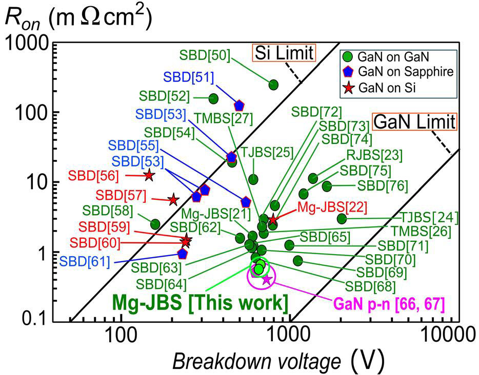
Figure 2: RON–BV benchmark comparison among GaN SBDs, Mg-implanted JBS, regrowth JBS (RJBS), trench JBS (TJBS), trench MOS barrier Schottky (TMBS), and p–n diodes (PNDs).
The BV2/RON figure of merit was 0.68GW/cm2 to 0.76GW/cm2, “one of the highest values reported so far for GaN SBDs,” according to the team (Figure 2). The low resistance values were maintained even when the termination structure was included in the normalization to give a total device area of 9.7x10⁻⁵cm2: 0.64mΩ-cm2 and 0.75mΩ-cm2 for A and B, respectively.
The author Mike Cooke is a freelance technology journalist who has worked in the semiconductor and advanced technology sectors since 1997.


