


News: Optoelectronics
2 December 2022
Monolithic GaN optoelectronics on silicon
Researchers in China and Japan have demonstrated a monolithic gallium nitride (GaN) optoelectronic system on silicon (Si) substrate consisting of a transmitter, modulator, waveguide, beam splitter, receivers and monitor [Hao Zhang et al, Appl. Phys. Lett., v121, p181103, 2022].
The team from China’s Nanjing University of Posts and Telecommunications and Zhengzhou University and Japan’s Nagoya University are seeking to promote optoelectronic systems with low power consumption while using monolithic integration on silicon to reduce material, processing and packaging costs.
The researchers comment: “We propose monolithic, top-down approaches to build III-nitride transmitter, modulator, waveguide, beam splitter, receiver and monitor as a single unit onto a conventional GaN-on-silicon wafer without involving regrowth or postgrowth doping.”
Apart from visible/ultraviolet light communication, the team sees opportunities in lab-on-chip setups.
The material for the device (Figure 1) was grown on 2-inch Si(111) with a GaN template layer. The buffer consisted of multiple layers of aluminium gallium nitride (850nm AlN/AlGaN) and 1030nm undoped GaN.
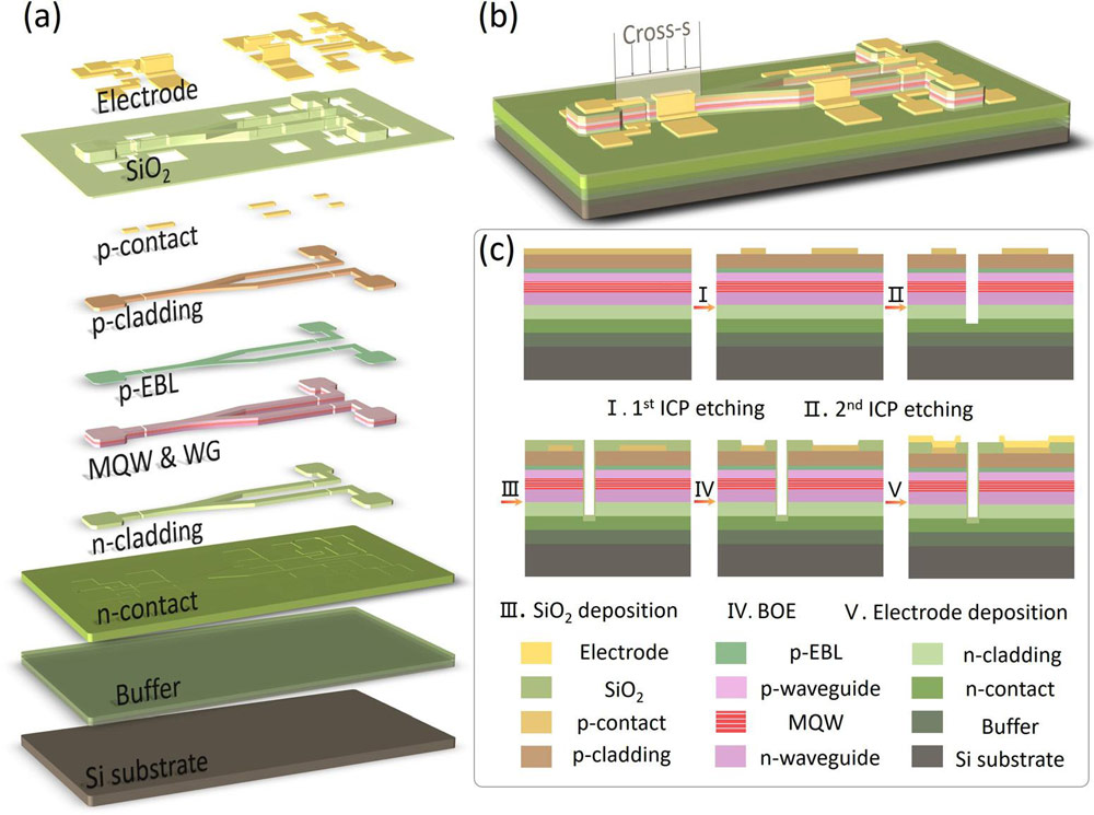
Figure 1: (a) Chip device layered structure. (b) Overview. (c) Manufacturing process flow.
The n-Al0.03Ga0.97N contact and n-Al0.1Ga0.9N/GaN superlattice cladding layers were 2450nm and 750nm, respectively.
The p-side had a 20nm p-Al0.25Ga0.75N electron-blocking layer (EBL), 500nm p-Al0.1Ga0.9N cladding layer, and 25nm p-GaN contact layer.
The inner undoped region had 80nm GaN waveguide, 59nm multiple-quantum well (MQW) active, and 60nm GaN waveguide layers before the EBL. The MQW consisted of 4x 3nm low-indium-content InGaN wells separated by 10nm Al0.08Ga0.92N barriers. The last barrier before the waveguide was 7nm.
The device fabrication used two inductively coupled plasma mesa etching steps of 200nm (p-contact) and 1.8μm (down to the n-contact) depths. The waveguide widths were 50μm. The Y-splitter angle was 30°. The electrodes consisted of titanium/platinum/gold. The electrical insulation was silicon dioxide (SiO2). The single emitter and two detector diodes were separated from the ends of the transmission waveguides by a gap of more than 6μm for better electrical insulation among the different devices and to improve weak signal detection.
Electroluminescence (EL) and responsivity spectra showed an approximate 14nm wavelength overlap with the response at shorter wavelength due to the Stokes shift. The EL peak was around 381nm. The response peak shifted noticeably under different reverse biases due to the quantum-confined Stark effect (QCSE) of the structure.
One test (Figure 2) consisted of the transmitter diode (T) being supplied with constant currents in a sequence, while electro-modulation of the light signal was provided by electrodes on the waveguide paths modulating the light absorption characteristic of the semiconductor structure: after the transmitter (M1) and in the two branches of Y-splitter (M2A/B).
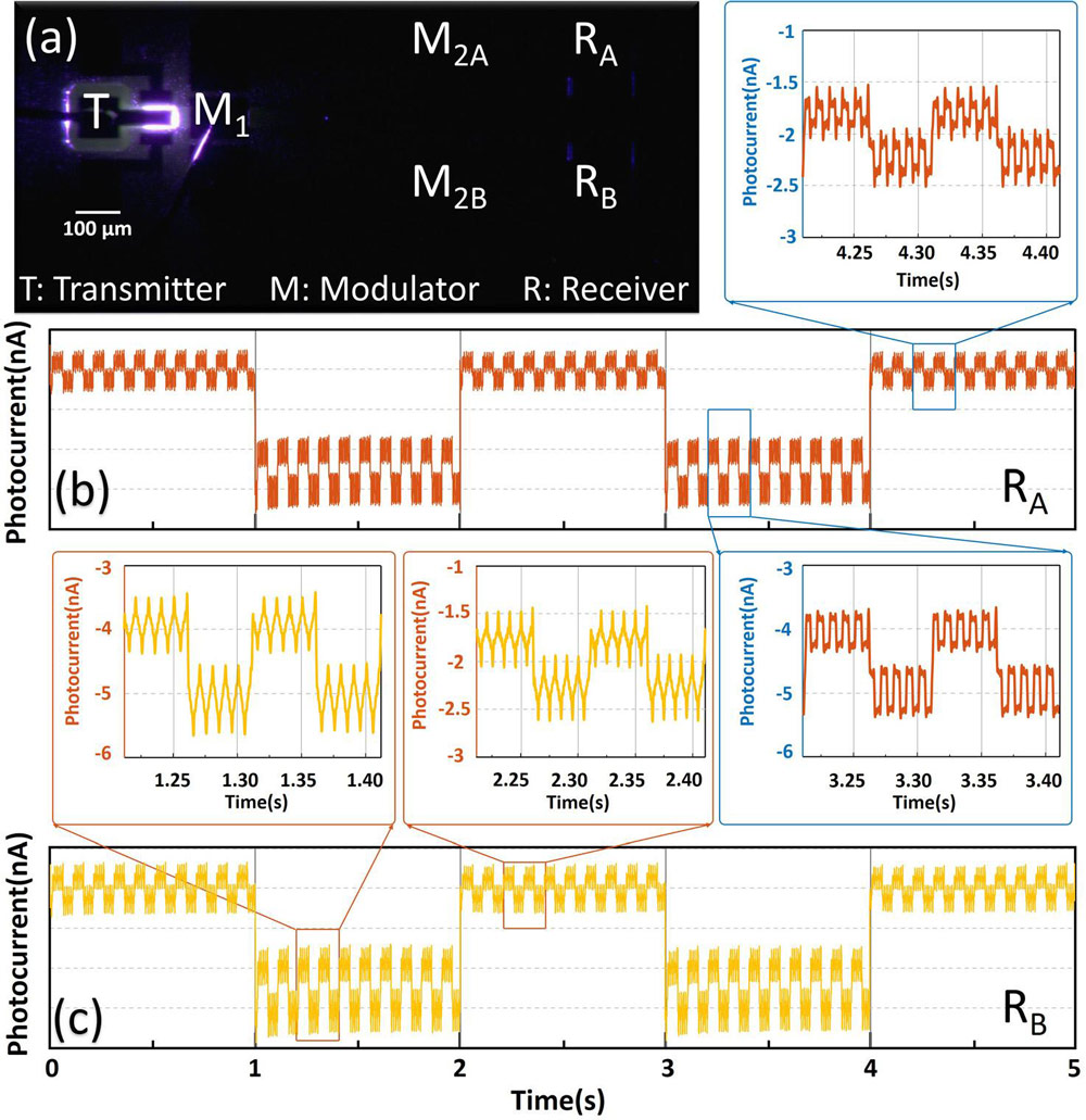
Figure 2: (a) Configuration of triple modulation on two paths. (b) Signals of receiver A (RA) and enlarged parts. (c) Signals of receiver B synchronized with receiver A.
The M1 signal was a 10Hz square wave, 6V peak-to-peak, with a -3V bias. The M2A branch was also square, modulated with 4V, -3V bias, at 100Hz, while the B-branch was modulated a triangular signal with the same peak-to-peak/bias voltages.
On the basis of ‘eye-diagram’ experiments with 50 megabit per second signals, the researchers believe that such data rates could be achieved with high-speed drive signals and detection circuits.
The author Mike Cooke is a freelance technology journalist who has worked in the semiconductor and advanced technology sectors since 1997.


