


News: Microelectronics
23 December 2022
Multi-dimensional wide-bandgap power devices
Three researchers based in the USA and the UK have reviewed the potential for applying multi-dimensional (multi-D) power device architectures with a view to suggesting more appropriate figures of merit (FOMs) compared with those applied to essentially 1D structures [Yuhao Zhang et al, Nature Electronics, v5, p723, 2022]. Such FOMs are key to assessing the performance limits and scaling capabilities of power devices.
The authors — Yuhao Zhang of Virginia Polytechnic Institute and State University (Virginia Tech), Florin Udrea of the University of Cambridge, and Han Wang of the University of Southern California — focus on multi-D structures pioneered in silicon in an effort to beat off the competition from potentially higher-power-capable but more expensive materials such as silicon carbide (SiC) and gallium nitride (GaN): superjunctions (SJs), multi-channels, fin field-effect transistor (FET), and trigate (Figure 1).
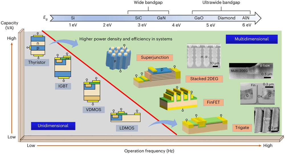
Figure 1: Power capacity and frequency trade-off of 1D and multi-D power devices: 1D — thyristor, IGBT, vertically diffused MOSFET (VDMOS) and laterally diffused MOSFET (LDMOS) — and multi-D. N- and p-type semiconductors, oxide and metal plotted in orange, blue, green and yellow, respectively. Circles represent electrodes. Included also scanning electron microscope cross-sections of multi-D devices.
For power devices one wants high voltages to be reached before breakdown in the off-state, while having low resistance to current flow in the on-state. These features are measured as the breakdown voltage (BV) and specific on-resistance (RON,SP), respectively (Figure 2). In addition, one usually wants the device to be ‘normally-off’ at zero gate potential, reducing power consumption and for fail safety.
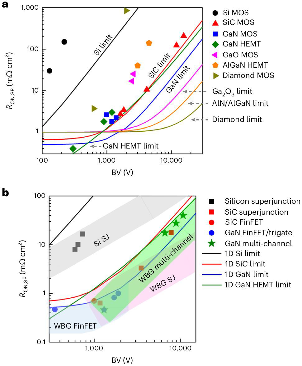
Figure 2: Specific on-resistance and breakdown voltage trade-off of reported 1D (a) and multi-D (b) power devices with theoretical limits.
One attraction of the new materials, such as GaN and SiC, is the potential reduction in device size, and increase in power density. Reduced size reduces the charge capacity (‘reduced parasitic capacitance’), allowing faster state changes (‘switching speed’). However, increased power density has implications for thermal management and packaging requirements.
The resistance consists of contributions from the ohmic contacts with the metal electrodes, the transistor/switch channel, and the drift region. The BV is limited by the critical electric field, which tends to increase as the square of the bandgap energy. At lower BV, the on-resistance is dominated by the channel. In wide-bandgap (WBG) and ultrawide-bandgap (UWBG) materials, the channel resistance is higher than desired. The effective channel mobility of SiC and GaN devices is in the range 130-150cm2/V-s, much lower than the 800-1200cm2/V-s bulk values. For UWBG materials such as aluminium nitride (AlN), gallium oxide (Ga2O3), and diamond, the channel mobility is even worse.
Meanwhile, drift regions need to keep the electric field below critical by ensuring the voltage drops over a sufficient distance. But the longer the distance, the higher the resistance to current flow in the on-state. Balancing the contradiction usually involves low doping. The on-resistance could be lowered with higher doping.
Superjunction structures enable this by balancing n-regions with p-type neighbouring material. In particular, the electric field becomes more uniform over the drift region, rather than peaking at the channel-drift junction. This enables higher voltage before breakdown.
Multi-channels can be viewed as a lateral form of the superjunction, using bandgap engineering rather than doping to achieve its effect. Although this lowers on-resistance, such a structure is more difficult to switch off due to the lower electrostatic control provided by the gate to the buried layers. Such control can be enhanced by using fin gates wrapping around the buried layers.
Another approach is the multi-channel monolithic-cascode high-electron-mobility transistor (HEMT), integrating a low-voltage single-channel enhancement-mode (normally-off) transistor with a multi-channel depletion-mode (normally-on) HEMT.
Having reviewed the present state of development, the authors conclude by offering some ideas of what the relevant performance parameters might be for future power devices based on multi-D superjunctions (Figure 3), and offering some complementary comments on radio frequency (RF) power amplifier devices.
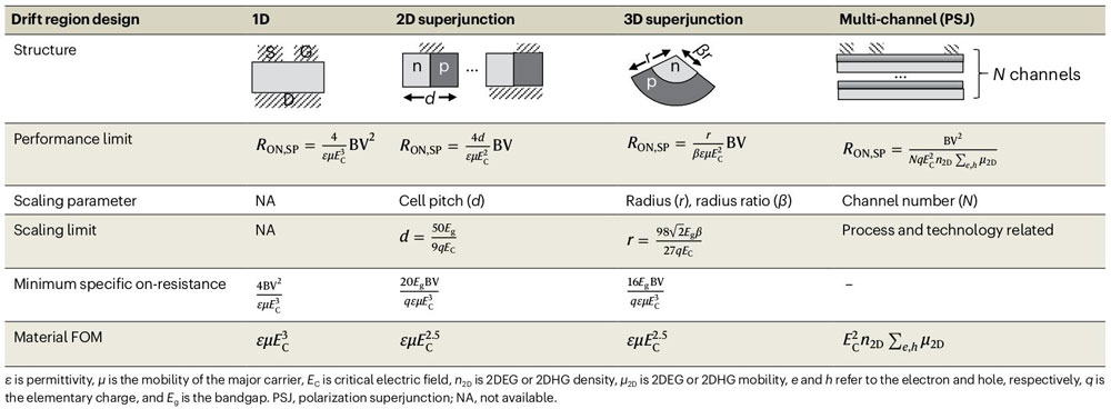
Figure 3: Performance limit, scaling parameter and limit, minimum specific on-resistance, and material FOM of 1D vertical unipolar devices, 2D and 3D superjunction devices and multi-channel lateral devices with precisely matched polarization charges.
For RF, one desires high-frequency, linear response in the multi-gigahertz range. The ability to reach RF is limited by parasitic capacitances. Linear response is particularly desirable for amplifiers aimed at new 5G wireless communications protocols.
The team reports: “Due to the presence of multiple channels, the transconductance (gm) of multi-channel HEMTs was found to exhibit broad plateau characteristics, which lead to higher device linearity.”
The author Mike Cooke is a freelance technology journalist who has worked in the semiconductor and advanced technology sectors since 1997.


