


News: Microelectronics
27 January 2022
Pushing indium phosphide DHBT frequency to 1.2THz
Switzerland’s ETH Zürich claims a record 1.2THz maximum oscillation frequency (fMAX) for a 0.25μmx0.44μm double-heterojunction bipolar transistor (DHBT) [Akshay M. Arabhavi et al, IEEE Transactions on Electron Devices, published online 6 January 2022] (see Figure 1). The materials used were a combination of indium phosphide (InP), gallium indium arsenide (GaInAs) and gallium arsenide antimonide (GaAsSb) with a staggered ‘type-II’ band alignment. This alleviates electron-blocking effects at the base–collector heterojunction.
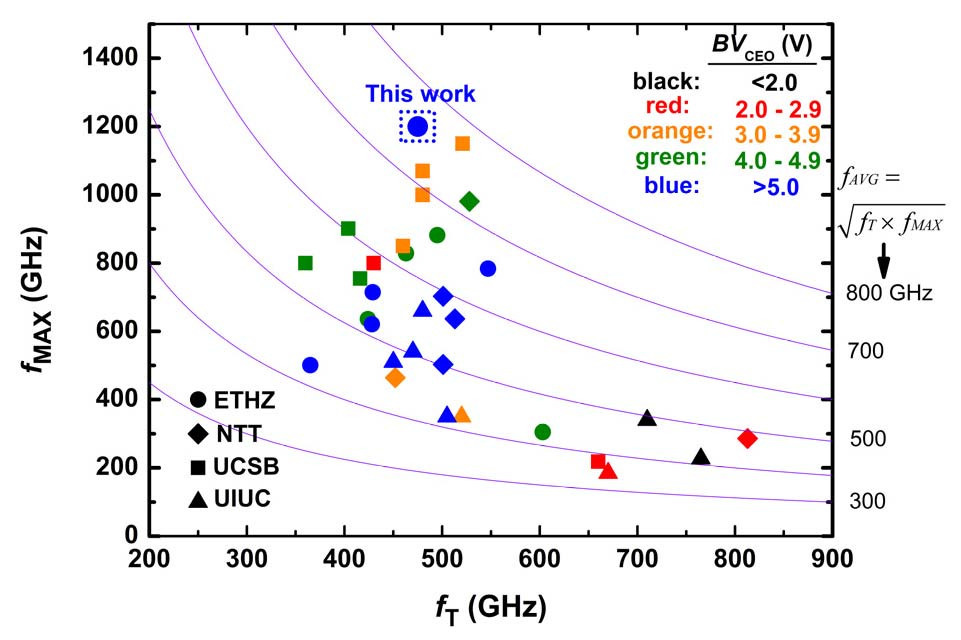
Figure 1: Survey of reported InP DHBT metrics. Breakdown voltages are color-coded.
The product of fMAX and open-base common-emitter breakdown voltage (BVCEO) of 6.48THz-V is also claimed to be the highest reported for any type of transistor. Even making the geometric average (square root of product) of fMAX with the 475GHz cut-off (fT) gives a InP DHBT record product with BVCEO) of more than 4THz-V. Gallium nitride high-electron-mobility transistors offer 4.9THz-V with a relaxed definition for breakdown voltage.
According to the team, these achievements result from:
- a tunable base–emitter access distance down to 10nm;
- the use of thicker base contact metals;
- minimization of parasitic capacitances and resistances via precise lateral wet etching of the base–collector (B/C) mesa.
The researchers comment: “The present scaling breakthrough, with the availability of THz transistors with larger junction areas capable of operation under high input drive and higher collector voltages, opens opportunities for the generation of significant signal power at mm-wave and sub-mm wave frequencies.”
The team sees oscillators and power amplifiers at these high frequencies as being more dependent on high fMAX rather than fT. The researchers also see the maintenance of high terahertz frequency performance to devices of 1.645μm2 area, more than 6x larger than previously reported THz InP DHBTs, as being an important achievement.
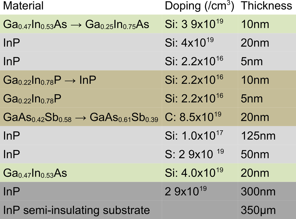
Figure 2: Semiconductor material structure.
The epitaxial semiconductor material (Figure 2) was prepared using metal-organic vapor-phase epitaxy (MOVPE) on 2-inch InP substrate. The gallium indium arsenide emitter layer was graded (Ga0.47In0.53As → Ga0.25In0.75As) to eliminate the conduction-band offset at the emitter–base (E/B) interface. The gallium arsenide antimonide base layer was also ramped (GaAs0.42Sb0.58 → GaAs0.61Sb0.39), along with the doping concentration.
Device fabrication began with forming the titanium/platinum/gold emitter electrode (Figure 3). Argon sputtering was used to etch the GaInAs emitter contact layer, while also smoothing the emitter electrode. Horizontal fins were added to the emitter electrode in processes involving a tri-layer photoresist, electron-beam lithography, and electron-beam evaporation and lift-off of the fin metal. The fins set the base access distance in a self-aligning manner.
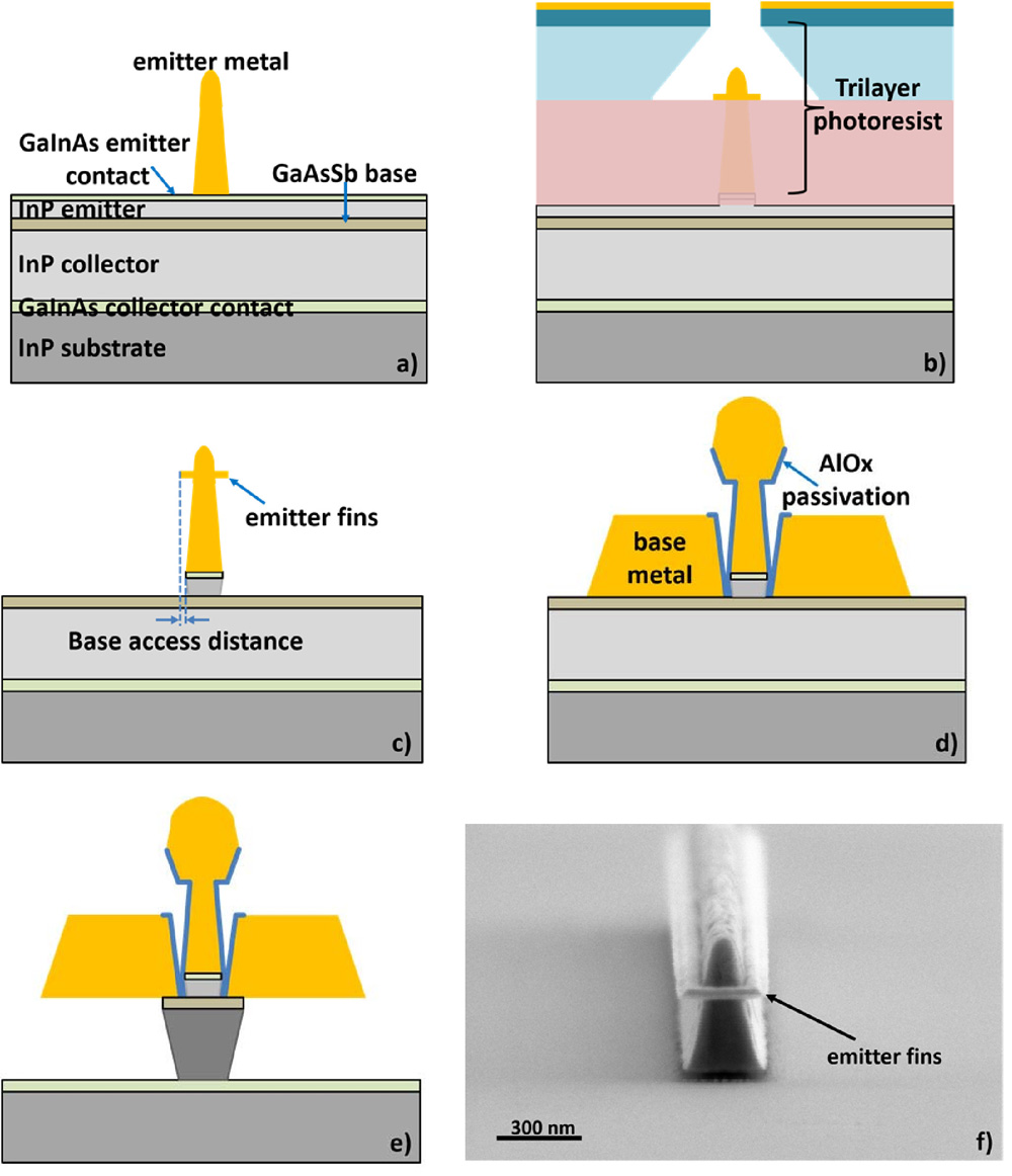
Figure 3: Simplified schematic view of key emitter fin fabrication steps: (a) emitter metal; (b) emitter fin formation using trilayer photoresist; (c) emitter mesa showing the base access distance; (d) self-aligned base contacts and AlOx passivation; and (e) narrow base–collector mesa. Schematics not to scale. (f) Scanning electron micrograph of emitter after mesa formation.
The emitter mesa was formed by phosphoric acid etch. The base region was then defined with electron-beam lithography, followed by electron-beam evaporation of palladium/nickel/platinum/gold. The fins allow a reduced base access distance to be combined with a thicker base metal layer (~50%) without shorting between the emitter/base contacts, reducing contact resistance. The surfaces of the base and emitter structures were then passivated with atomic layer deposition (ALD) of aluminium oxide (AlOx).
A sequence of dry and wet etches were used to give an undercut collector mesa with an effective base–collector contact width of 40nm. This distance ensures that “only a transfer length equivalent of base material remains under the base metal contact,” the team comments.
The device was planarized using a Teflon-based process and completed with electron-beam evaporated coplanar probe pads.
The open-base common-emitter breakdown voltage BVCEO was 5.4V at a collector current density of 1kA/cm2. Single-pole extrapolations from Mason’s unilateral power gain and common-emitter short-circuit current-gain small-signal radio frequency (RF) measurements up to 50GHz gave peak maximum oscillation (fMAX) and cut-off (fT) frequencies of 1.2THz and 475GHz, respectively, with 1V collector–emitter bias (VCE).
A single-finger (0.175μmx9.4μm) DHBT biased for class-A operation was subjected to active-loop load-pull continuous wave (cw) large-signal measurements at 94GHz. The power-added efficiency (PAE) was 32.5% (40% collector efficiency) with 1.6V VCE bias and 1mA base current (IB). The saturated output power (Pout,sat) was 8.73dBm and the gain 7.8dB.
Increasing VCE to 1.9V enabled a higher peak Pout,sat at the expense of lower PAE: 10.4dBm (832mV VBE) and 29.3%, respectively. The Pout,sat density was 6.67mW/μm2, or 1.7W/mm according to emitter length.
The device was found to operate stably at the large VCE bias with no evidence of degradation. “Such device stability under aggressive large-signal operation suggests inherent reliability advantages in the InP–GaAsSb material system,” the team comments.
The measurements were made without thermal management enhancements such as substrate thinning and/or transferring the devices to thermally conductive substrates, e.g. aluminium nitride or silicon carbide.
https://doi.org/10.1109/TED.2021.3138379
The author Mike Cooke is a freelance technology journalist who has worked in the semiconductor and advanced technology sectors since 1997.


