


News: Optoelectronics
20 January 2022
University of Surrey produces record strain in single-crystal silicon
University of Surrey researchers have developed a single-step procedure to put single-crystal silicon under more strain than has been achieved before (Mateus G. Masteghin et al, ‘Stress-strain engineering of single-crystalline silicon membranes by ion implantation: Towards direct-gap group-IV semiconductors’, Phys. Rev. Materials 5, 124603). The discovery (which has a patent pending) could be crucial to the future development of silicon photonics, it is reckoned, which is currently constrained by the lack of cheap, efficient and easily integrated optical emitters.
Now, the Surrey-based researchers are transferring the same procedure to germanium. If successful, they could open the door to creating germanium lasers, which are compatible with silicon-based computers, and could yield new optoelectronic devices for communications systems. This would address the problem of overheating, which is becoming a threat to development in silicon-based computer systems, and would eliminate the need to develop expensive and difficult-to-integrate III-V devices (a popular area of research to try to overcome overheating).
Moving photonics fully onto silicon has been a long-held goal. While there have been many successes in developing passive silicon photonic devices, a laser that is CMOS-industry compatible, using elements from the same group of the periodic table, has remained elusive until now. The team was recently awarded a New Horizons project grant by the UK Engineering and Physical Sciences Research Council (EPSRC) to exploit their innovation and progress their work.
The new approach is also an important step towards creating near-infrared sensors that could pave the way towards developing more sophisticated smartphones – e.g. fitting them with fire alarms and carbon monoxide sensors.
The new paper in Physical Review Materials describes how the team generated strain via ion implantation in suspended membranes in a similar manner to tightening a drum skin. The effect is created by a downward bowing of the implanted region because of a still crystalline layer beneath the implanted, amorphized top region in a mechanism analogous to a bi-metallic strip submitted to a temperature change.
The team from the University of Surrey’s Advanced Technology Institute and Department of Physics demonstrated (using micro-Raman spectroscopy) that up to 3.1% biaxial tensile strain and up to 8.5% uniaxial strain can be generated, but they point the way to even larger strains, achievable by varying the implant species and by exploiting the underlying crystal direction.
The method far exceeds previous records using more complex approaches. In the group-IV semiconductor germanium, an indirect-to-direct transition in the electronic bandgap occurs at much lower strains than silicon, where this new method offers huge potential.
Although the procedure is relatively simple and points the way to a versatile, fast, generally applicable and widely available technique for strain control, its development required the use of two national facilities: the Surrey Ion Beam Centre (which allows users to undertake a wide variety of research using ion implantation, ion irradiation and ion beam analysis, and which also has extensive processing and characterization facilities) and the National Physical Laboratory (the UK’s National Metrology Institute, which develops and maintains national primary measurement standards and which ensures that cutting-edge measurement science has a positive impact in the real world).
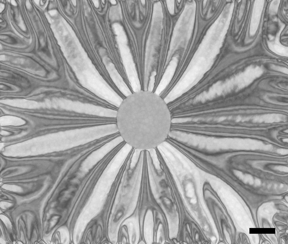
Picture: This experiment helped to understand the effect of ion beam implantation on thin single-crystal membranes by creating an analogy with a liquid droplet placed on a thin elastic membrane in which its weight creates a downward bending (bowing) of the film beneath the droplet, followed by the appearance of radial wrinkles. The scale bar corresponds to 10µm. (Image: University of Surrey).
“What excites me about this is the simplicity of the method and that it can easily be transferred to production methods,” says Dr David Cox, senior research fellow at the Advanced Technology Institute at the University of Surrey. “It will be exciting to see if this can have as significant an impact on group-IV semiconductor photonics as Alf Adam’s long-standing legacy on the development of the strained-layer III-V-based quantum-well lasers. Photonics will be to the 21st Century what electronics was to the 20th Century: revolutionary,” he reckons.
“Seeing the wrinkles annihilation and the flattening of the membranes in real time was astonishing,” says Ph.D. student Mateus Masteghin, lead author of the study. “This new technique promises to be highly disruptive to the field of photonics, and I am looking forward to continuing developing new devices based on this proposed technique.”


