News: Microelectronics
28 July 2022
Lateral polarization GaN HEMTs
Researchers based in China and Saudi Arabia propose lateral modulation of the charge polarization of III-nitride material as a more effective route to electrically isolate high-electron-mobility transistors, compared with mesa etching or ion implantation [Yijun Dai et al, Appl. Phys. Lett., v121, p012104, 2022].
Current leakage occurs in mesa etched structures through surface damage. Ion implantation needs high-temperature annealing to repair crystal structures, which can result in poor thermal stability and introduction of deep-level defects.
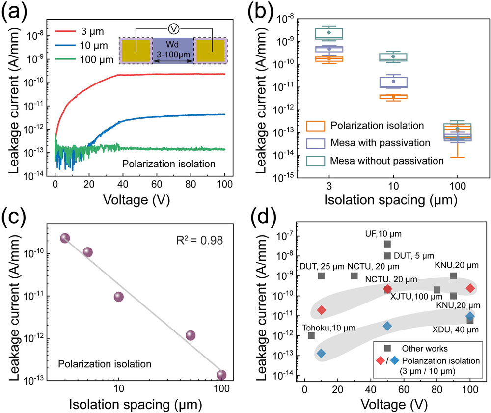
“Structures of polarization-isolated high-electron-mobility transistors (PI-HEMTs) exhibit significantly reduced isolation leakage currents by up to nearly two orders of magnitude at 50V voltage bias compared to the state-of-the-art results,” the team from Ningbo Institute of Materials Technology and Engineering and University of Chinese Academy of Sciences, China, and King Abdullah University of Science and Technology (KAUST), Saudi Arabia, comment.
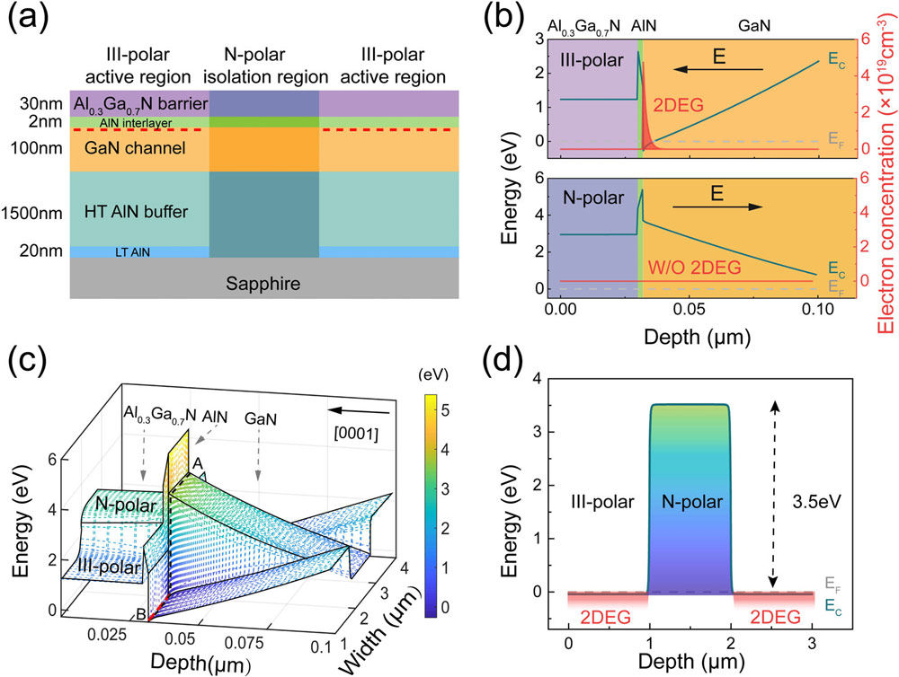
The PI-HEMTs used a lateral polarity structure (LPS) with N-polar material providing isolation between III-polar HEMT regions (Figure 1). The two-dimensional electron gas (2DEG) at the aluminium gallium nitride (AlGaN) barrier/gallium nitride (GaN) channel interface usual in III-polar structures is expected in the N-polar isolation regions to be depleted owing to the Fermi level being below the conduction band.

Figure 1: (a) Cross-sectional PI-HEMT scheme. Red dashed line represents 2DEG. (b) Band diagrams. (c) Three-dimensional mapping of conduction band showing barrier height between III- and N-polar GaN of PI-HEMT structure with 1μm N-polar width (i.e. isolation spacing). (d) Conduction band diagram extracted from dashed line A-B in (c).
“Due to inversion of the spontaneous polarization direction, the polarization-induced electric field in the III-polar structure is opposite to that of the N-polar structure,” the researchers explain.
The N-polar material therefore can be used to electrically isolate the III-polar 2DEG. The team estimates the induced barrier height at 3.5eV, “significantly larger than the conduction-band offset between AlN and GaN”.
The team sees their work as potentially leading to GaN power electronic arrays and monolithic microwave integrated circuits (MMIC) with high breakdown voltage and high-density chip integration. Enhanced isolation will enable GaN technology to leverage the full benefit of its high breakdown voltage, fast switching speed, and continued operation at high temperature (HT).
Other devices that could benefit from LPS include super-junctions, Schottky barrier diodes (SBDs), MESFETs, and photodetectors.
The sources for metal-organic chemical vapor growth of the HEMT material on 2-inch sapphire were trimethyl-Ga/Al and ammonia (NH3).
The PI-HEMT material growth differed from the usual HEMT process by using a patterned rather than uniform 20nm low-temperature AlN nucleation layer. Care was taken to apply identical surface pre-treatments to the PI-HEMT nucleation layer and a reference regular HEMT structure, grown with uniform AlN nucleation.
The material on AlN nucleation was III-polar, while that on the bare sapphire was N-polar. The transition between the materials was of the order of a few nanometers, according to high-resolution transmission electron microscope analysis.
The III-polar structure resulted in a 2DEG with 1.5x10¹³/cm2 carrier concentration and 1277cm2/V-s, and 326Ω/square sheet resistance.
The team reports: “Due to the large lattice mismatch between the GaN channel and AlN buffer, the quality of the GaN channel layer is deteriorated, leading to scattering effects and reduced carrier mobility.”
The PI-HEMT was fabricated by electron-beam evaporation and annealing of titanium/aluminium/nickel/gold source/drain electrodes and nickel/gold gate deposition.
The isolation performance was measured between two HEMT III-polar regions separated by 100μm, 10μm and 3μm N-polar regions. The applied bias reached up to 100V. For PI, the isolation leakage was fairly steady above 40V. The 100μm leakage was of the order 10-13A/mm at 40V and above. Reducing the gap increased the current to 2x10-12 and 2x10⁻¹⁰A/mm, respectively, for the shorter 10μm and 3μm gaps.
Comparison was made with uniform HEMT regions, isolated with the usual plasma etching process to a depth of 120nm. Some of these samples also were treated with hydrogen chloric acid passivation. These had a similar isolation performance to the PI samples with 100μm gaps. However, differences became apparent for the shorter gaps with the PI sample significantly outperforming both the mesa structure with and without passivation (Figure 2).

Figure 2: (a) Leakage versus voltage for PI-HEMT structures. (b) Comparison of PI- with mesa-isolated III-polar HEMT structures with various isolation spacings at 100V bias; (c) leakage versus isolation spacing of PI-HEMT at 100V bias. (d) Benchmarking of leakage versus voltage against state-of-the-art results.
The improved isolation of the PI-HEMT structure led to an expected enhancement of the two-terminal breakdown characteristics. The breakdown for the PI-HEMT structure with 3μm isolation was 2680V, compared with 1380 and 1644V for mesa isolation without and with passivation, respectively.
Increasing the isolation width to 10μm gave breakdowns below 3000V for the mesa isolations, while the PI structure did not suffer breakdown at this level. No breakdown was observed at 3000V for any of the samples with 100μm isolation. “The results suggest that the polarization isolation is highly advantageous in high-density high-power device integration,” the team observes.
The 3μm gate-length PI-HEMTs had a rather negative threshold (normally-on/depletion-mode) of -6.1V. The researchers see this as being mainly due to the thick 30nm AlGaN barrier. The source-gate and gate-drain distances were 2 and 3μm, respectively.
The off-state leakage was ~2x10⁻⁸mA/mm, giving an on/off current ratio of order 109. The off-state was dominated by gate leakage current. The subthreshold slope was 61mV/decade, close to the theoretical minimum of 60mV/decade.
The researchers comment: “The result unambiguously demonstrates the excellent leakage suppression of the PI-HEMT device, revealing the unique advantage of utilizing polarization modulation to tune the 2DEG in-plane.”
https://doi.org/10.1063/5.0097037
The author Mike Cooke is a freelance technology journalist who has worked in the semiconductor and advanced technology sectors since 1997.


