


News: LEDs
30 June 2022
Full-color μLED pixels for displays and optical near-field communication
Researchers based in China report on all-in-one micro-light-emitting diode pixels (μLEDPs) with integrated red-green-blue super-pixels (RGBSPs) aimed at simultaneous display and optical near-field communication (ONFC) capability [Xinyi Liu, et al, Optics Express, v30, p24889, 2022].
“To the best of our knowledge, the proposed integrated μLEDP achieves the highest data rate compared to published results based on other multi-color, low-capacitance, high-bandwidth LEDs,” reports the team from Hong Kong University of Science and Technology, Southern University of Science and Technology, and HKUST Shenzhen-Hong Kong Collaborative Innovation Research Institute.
The researchers also see potential for the μLEDPs in general lighting applications based on a wide range of color temperatures from warm to cool white.
The researchers fabricated 100μmx200μm RGBSPs.
The red super-pixels (Figure 1) were created from aluminium gallium indium phoshide (AlGaInP) multiple quantum wells (MQWs) on gallium arsenide (GaAs) substrate by metal-organic chemical vapor deposition (MOCVD). The material was then glued to sapphire and the growth substrate removed by wet etching.
The device mesa was formed using inductively coupled plasma (ICP) etch with silicon dioxide (SiO2) hard mask. The cathode consisted of 200nm gold/germanium/nickel (Au/Ge/Ni) on the n-GaP contact layer, and the anode was 200nm gold/zinc (Au/Zn) on the p-GaP layer. Plasma-enhanced CVD SiO2 was used as a 600nm passivation layer. The n- and p-contact pads were electron-beam evaporated indium.
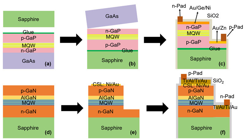
Figure 1: (a-f) Fabrication process flow of AlGaInP red super-pixel (top) and InGaN green/blue super-pixel (bottom) in proposed all-in-one μLEDP.
The green and blue super-pixels used MOCVD indium gallium nitride (InGaN) MQWs on sapphire. The mesa was again formed by ICP etching. A 10nm layer of Ni/Au was then evaporated on the p-GaN contact material as a current-spreading layer (CSL). The CSL was subjected to rapid thermal annealing to ensure an ohmic contact behavior.
The n- and p-electrodes consisted of titanium/aluminium/titanium/gold (Ti/Al/Ti/Au). The pad metal was again indium, applied after the deposition of SiO2 passivation.
The μLEDP was assembled and packaged by first applying solder bumps to the devices and then singulating the wafers using laser cutting. The RGBSPs were individually transferred and flip-chip bonded at 50μm pitch onto a circuit with a common p-pad. Black silicone was used as encapsulation to improve the contrast ratio. The final device measured 0.79mmx0.79mmx0.65mm (Figure 2).
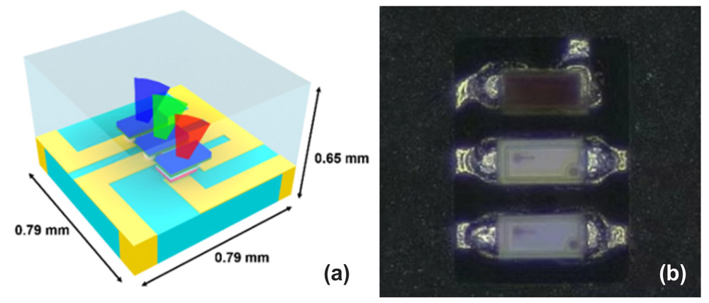
Figure 2: (a) 3D perspective view of μLEDP internal package structure. (b) Microscope image.
The 10-4A/cm2 turn-on voltages were 1.44, 2.00, and 2.33V for the RGB sub-devices, respectively. The peak light powers were 1.86/2.08/4.33mW, recorded respectively in the same order at 20/55/55mA current injection.
The spectral performance of the RGB devices showed peaks at 640nm, 515nm and 463nm, respectively, with full-widths at half-maximum (FWHM) of 23nm, 38nm and 28nm. The devices were biased to give 30mA, 55mA and 55mA injection, respectively, for these measurements.
The color gamut of the RGB combination was 109% of the NTSC standard used for analog color TV. Apart from display applications, the device could also meet demands for smart lighting with correlated color temperatures (CCTs) ranging between 2831.7K and 10016.8K – warm through neutral to cool white.
The RGB bandwidths for ONFC derived from S-parameter measurements were 62MHz, 58MHz and 61MHz at 45mA, 70mA and 75mA injection, respectively. The team considers these values to be sufficient for practical ONFC systems. The known parasitic effects of the PCB test fixture and packaging suggest the intrinsic bandwidths were more than 100MHz.
The researchers comment: “The modulation bandwidth of RGBSPs in this report still has room to be improved due to the limitation of transferring sub-pixels from different substrates. The size of RGBSPs was chosen based on the consideration of display and communication link performance.”
Bit-error rate (BER) testing with pseudo-random binary sequences showed that data rates up to 220, 170 and 195Mbits/s for RGB, respectively, could be reached without breaking the forward-error correction (FEC) limit of 3.8e-3. The data rates for 10e-9 BER were 201/148/179Mb/s, respectively.
The researchers also developed a compact equivalent circuit model of the device to enable the exploration of various data modulation schemes in simulation such as non-return to zero (NRZ) and 4-level pulse amplitude modulation (PAM-4). The maximum simulated data rates for these schemes were 0.3Gb/s and 1.1Gb/s, respectively.
Micro-light-emitting diode pixels InGaN GaAs substrate AlGaInP MOCVD
https://doi.org/10.1364/OE.461762
The author Mike Cooke is a freelance technology journalist who has worked in the semiconductor and advanced technology sectors since 1997.


