


News: LEDs
15 June 2022
Stabilizing colors for micro-displays
The UK’s University of Sheffield has used a simple micro-cavity structure to create micro light-emitting diodes (μLEDs) with a stable emission wavelength over a range of injection currents [Guillem Martinez de Arriba et al, ACS Photonics, published online 27 May 2022]. Such wavelength stability is one of the key requirements for one of the projected applications of μLEDs: full-color micro-displays for augmented reality (AR)/virtual reality (VR) imaging.
Indium gallium nitride (InGaN) LEDs suffer from large wavelength shifts with current for a variety of reasons, with one of leading causes being the quantum-confined Stark effect (QCSE). The Stark effect refers to a shift in energy in the presence of electric fields. Applying a bias to the structure changes the electric field and hence shifts the emission wavelength.
In InGaN LEDs charge polarization of the chemical bonds leads to spontaneous and strain-dependent electric fields in the material even at zero bias. As the indium content of the light-emitting regions of such devices increases to enable longer-wavelength LEDs, the InGaN suffers from increasing strain relative to the base GaN material of its surroundings. Moving to semi-polar or non-polar orientations of the GaN crystal structure does not significantly improve color stability.
The Sheffield approach to stabilizing the wavelength was to create a Fabry-Perot optical cavity that selected a stable wavelength from the μLED (Figure 1). The cavity was formed between a distributed Bragg reflector (DBR) and the top interface with the air. The team comments: “This approach provides a simple solution to resolving the 30-year issue in the field of III-nitride optoelectronics.”
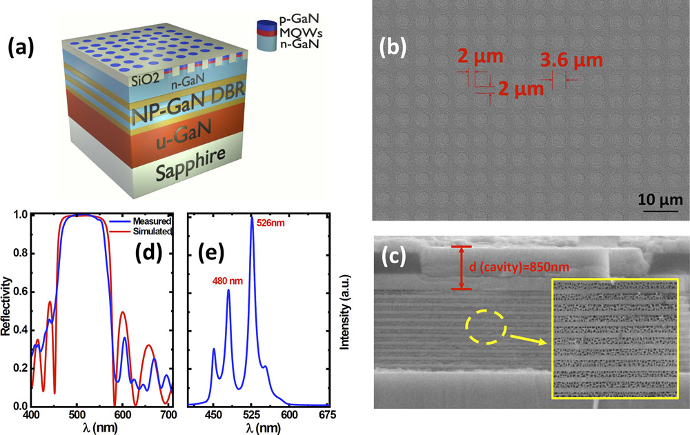
Figure 1: Schematic of μLEDs with bottom NP GaN DBR with lattice matching (a); (b) plane-view scanning electron microscope (SEM) image of regularly arrayed μLED epiwafer with 3.6μm-diameter devices at 2μm; interpitch (c) cross-sectional SEM image of NP-GaN/undoped GaN DBR (inset: zoomed image); (d) reflectance spectra of NP GaN DBR and FDTD simulated results; (e) mode spectrum, which is obtained by using the 3D FDTD simulations to confirm the existence of optical modes.
The DBR was formed from the large refractive index contrast between solid and nanoporous (NP) GaN layers. The nanoporosity was achieved by an electrochemical (EC) etch process.
The NP-GAN DBR was fabricated on an undoped GaN template on sapphire, created using a two-step metal-organic vapor phase epitaxy (MOVPE) process. The DBR region material consisted of 11 pairs of alternating heavily n++-doped (1019-1020/cm3) and undoped GaN.
The initial material was completed with a 300nm n-GaN (5x10¹⁸/cm3) layer and 500nm plasma-enhanced chemical vapor deposition (PECVD) silicon dioxide (SiO2).
The top SiO2 dielectric layer was punctured with an array of circular holes by inductively coupled plasma etch. The μLEDs were formed using MOVPE selective epitaxial overgrowth in these holes. This avoided the usual plasma etch normally used to fabricate μLED, which tends to create sidewall damage, resulting in increased current leakage.
The LED layers were n-GaN contact, In0.05Ga0.95N pre-layer, 5x(2.5nm InGaN/13.5nm GaN) multiple quantum well, 20nm aluminium gallium nitride electron-blocking layer, and 200nm p-GaN contact. The total thickness of the LED structure came to an approximate level with the 500nm SiO2 dielectric.
The NP-GaN was then formed from the electrically conductive n++-GaN layers being subjected to EC etching. The reflectance properties of the resulting material showed a 122nm stop-band around a central wavelength of 520nm, matching the designed performance from finite-difference time-domain (FDTD) simulations.
The DBR formed an effective cavity length for the μLEDs of more than 1μm (850nm physical + electric field penetration into the DBR). The researchers estimated the refractive index of the NP-GaN at 1.75, based on an observed 0.6 porosity. The refractive index of solid GaN is around 2.3.
The EC process used an indium anode, platinum cathode, and 0.3 molar concentration nitric acid solution. The EC bias was 5.5V.
The μLED material with and without being subjected to EC etching was fabricated into 330μmx330μm devices with indium tin oxide (ITO) transparent conductor on the p-GaN and titanium/aluminium/nickel/gold metal for the n-contact. The electrodes were titanium/gold. No extra measures were applied to enhance light extraction such as optical coatings, passivation, epoxy encapsulation, or reflectors.
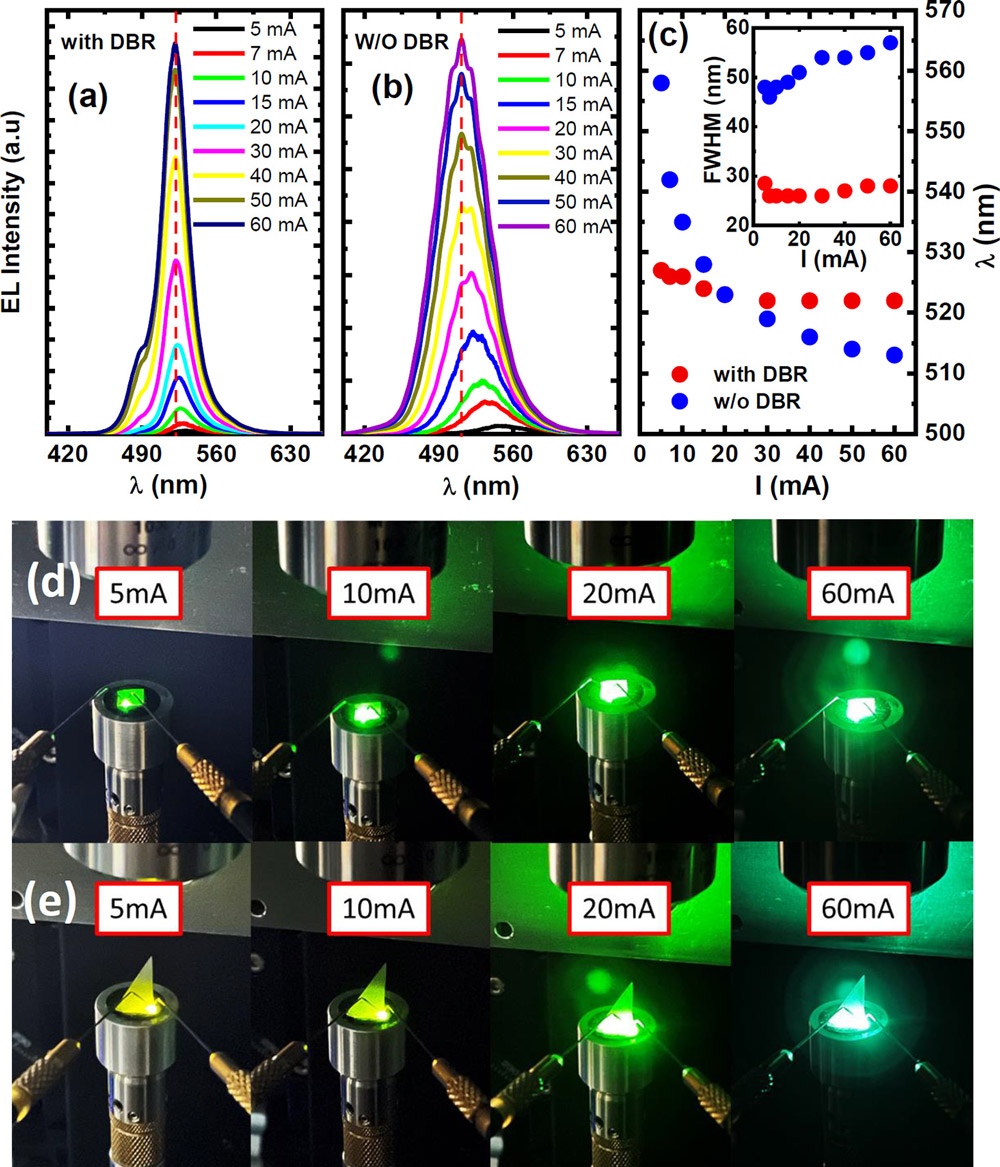
Figure 2: Electroluminescence (EL) spectra μLEDs with (a) and without (b) DBR as function of injection current; EL emission wavelength and full-width half-maximum (FWHM) of EL spectra versus injection current (I) (c); EL emission images of μLEDs with DBR (d) and without DBR (e) as function of injection current.
While the μLEDs without DBR (Figure 2) show a strong shift in wavelength with increased injection current (560-510nm for 5-60mA increase), the device with DBR shows a relatively stable emission (less than 10nm around 525nm). Also, the DBR narrows the spectral line by about half. “Only at a high injection current, a weak shoulder at 480nm appears due to the second optical mode,” the team explains.
Visibly, while the DBR μLED has a stable green emission throughout the injection range, without the DBR there is a clear transition through yellow, yellow-green, green, and ending up at blue-green. This region of the spectrum is the one to which the human eye is most sensitive to color changes.
The researchers comment: “Such a blue-shift in emission wavelength with increasing injection current is the fingerprint of QCSE. Such μLEDs cannot be used for the fabrication of a micro-display. In contrast, the μLEDs with DBR constantly emit green light throughout all the injection current.”
The author Mike Cooke is a freelance technology journalist who has worked in the semiconductor and advanced technology sectors since 1997.


