News: LEDs
30 March 2022
N-polar InGaN LEDs with record output power
University of California Santa Barbara (UCSB) in the USA claims record high power of up to 0.21mW at 20mA current injection for nitrogen-polar indium gallium nitride (InGaN) LEDs grown by metal-organic chemical vapor deposition (MOCVD) [Vineeta R. Muthuraj et al, Appl. Phys. Lett., v120, p101104, 2022]. The devices produced blue to blue-green light with wavelengths between 470nm and 506nm.
Although Ga-polar devices generate higher light output power, there are a number of properties of N-polar material that could be handy in future development. For starters, N-polar GaN more easily incorporates indium, potentially allowing longer wavelengths to be reached. In addition, charge transport is better, offering opportunities to reduce efficiency droop at high current injection. Unfortunately, up to now N-polar devices have only managed up to 20μW at 20mA injection.
Another unusual feature of the UCSB devices was the use of an inverted structure with the p-type layers buried underneath the light-emitting quantum wells (QWs). This allows better quality p-GaN to be grown at a higher temperature, but creates problems for activating the magnesium (Mg) doping, which is passivated by hydrogen, impossible to avoid in MOCVD processes. Vias were drilled by etching into the material to allow hydrogen to escape during thermal annealing from the buried p-GaN layers.
The normal p-GaN-on-top structure is restricted in growth temperature by the imperative not to thermally degrade the underlying InGaN QWs. The resulting p-GaN material tends to have a high resistance to current flow. In the inverted structure, relatively low-resistance n-GaN can be achieved with a lower growth temperature.
Electrical power to inject holes into the QW active region was supplied through a thin tunnel junction with n-type material.

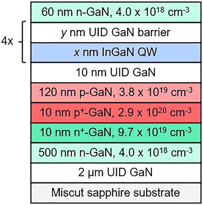
Figure 1: Epitaxial structure of inverted N-polar LED with doping levels obtained from secondary-ion mass spectrometry (SIMS).
The N-polar material (Figure 1) was grown on 4° misoriented sapphire. The metal-organic precursors were trimethy- and triethyl-Ga and trimethyl-In. The silicon (Si) and magnesium (Mg) dopants were sourced by disilane (Si2H6) and bis-cyclopentadienyl Mg (Cp2Mg), respectively. The nitrogen came from ammonia (NH3).
The light-emitting quantum wells (QWs) consisted of InGaN of thickness between 1.5nm and 4.5nm and GaN barriers between 7nm and 15nm.
The initial unintentionally (UID) and n-type doped GaN layers were grown at 1200°C. The temperature was reduced to 800°C for the heavily doped n+-GaN tunnel-junction layer, and then raised to 1080°C for the p-type layers and the 10nm UID GaN spacer. The wells were grown at 800°C, and the barriers at 830°C. The final 60nm n-GaN was produced at 900°C.
The LED fabrication began with mesa and activation via reactive-ion etch using silicon tetrachloride (SiCl4), followed by buffered hydrofluoric acid and ultraviolet ozone treatments. The device area was 0.1mm2.
The circular activation vias were 3μm diameter in a square array. The center-to-center distance was 6.5μm. The activation itself consisted of 700°C rapid thermal annealing for 30 minutes.
Aluminium/nickel/gold were used for the contacts to the n-GaN of the top and bottom of the device.
The electroluminescence spectra were single-peaked with a shoulder on the short-wavelength side being attributed to “a combination of InGaN alloy compositional fluctuations and thickness fluctuations in the quantum wells”.
A blue LED with 1.5nm/11nm wells/barriers had a 470nm peak wavelength with 40nm full-width at half maximum (FWHM) at 20mA DC injection. The wavelength and FWHM were fairly stable in the range 5-100mA with most-likely self-heating counteracting blue-shift effects. The self-heating was the result of lower efficiency relative to Ga-polar devices. The light output power of the brightest device at 20mA was 0.21mW. The peak power was 0.97mW at 244mA.
The turn-on voltage was high at ~6V. “The excess voltage may be explained by incomplete activation of the Mg dopants in the buried p-GaN layers,” the team explains. The researchers suggest micro-LED formats and improvement of the tunnel-junction structure could reduce the voltage. Micro-LEDs have increased area for the escape of hydrogen during activation.
The external quantum efficiency (EQE) peaked around 5A/cm2 injection current density. The EQE dropped by 37% when the density reached 100A/cm2. The researchers comment: “Previously published N-polar LED EQE data showed 33% droop with integrated EQE measurements going up to only 12A/cm2.”

Figure 2: Electroluminescence wavelength and light output power versus (a) quantum well thickness with 11nm wide barriers and (b) barrier thickness with 1.5nm wide quantum wells. Wavelength points labeled with FWHM in nanometers.
The devices with varied well and barrier thicknesses enabled emission wavelengths of 506nm to be reached under 20mA (20A/cm2) DC injection (Figure 2).
SIMS studies showed oxygen and carbon impurity levels comparable to or higher than previous work on N-polar devices with 6μW-level light output power. The team comments: “With impurities being a less likely factor in poor N-polar luminescence, the primary reason for the improvement in this work is most likely the growth of the p-GaN layers at high temperature, which was enabled by the inverted structure.”
N-polar InGaN LEDs InGaN LEDs MOCVD
https://doi.org/10.1063/5.0083893
The author Mike Cooke is a freelance technology journalist who has worked in the semiconductor and advanced technology sectors since 1997.


