


News: Optoelectronics
12 May 2022
InGaAs/AlGaAS nanowires on silicon
Researchers based in Russia report on molecular beam epitaxy (MBE) of indium gallium arsenide (InGaAs) quantum dots/wires (QDs/QWs) in aluminium gallium arsenide (AlGaAs) nanowires (NWs) on silicon (Si) “for the first time” [Rodion R. Reznik et al, Phys. Status Solidi RRL, p2200056, 2022].
The research team at St. Petersburg State University, Alferov University, Institute for Analytical Instrumentation RAS, Ioffe Physical Technical Institute RAS, and National Research University Higher School of Economics, have previously studied MBE synthesis of GaAs QDs inside AlGaAs nanowires on silicon.
The researchers comment that these hybrid nanostructures were effective sources of single photons in a wavelength range of 750–800nm. Thus, they constitue “promising candidates for use in quantum cryptography and alkali metal (e.g. rubidium or cesium)-based atomic clock adjustments.”
The replacement of GaAs by InGaAs allows access to longer wavelength, including those in the important telecommunication optical fiber range of 1.3μm. Such wavelengths can also be transmitted through waveguides formed in the silicon substrate itself.
The team writes: “Our work, therefore, opens up new prospects for the integration of direct-bandgap semiconductors with the silicon platform for various applications in the fields of silicon photonics and quantum communication technology.”
There have been previous reports of InGaAs/GaAs nanowires, but grown on GaAs rather than silicon substrates, and photoluminescence emissions only presented at low temperature.
Similar QD/QW formations have been studied in the indium arsenide phosphide (InP/InAsP) system. However, phosphorus tends to be tricky to handle in a safe, controlled manner during MBE growth.
The researchers comment: “The results of both optical and structural properties studies of grown structures showed that, similar to the case of the InP/InAsP system, radial InGaAs QWs in addition to InGaAs QDs are formed inside the nanowires as a result of lateral and axial InGaAs growth competition.”
The nanowires were grown by MBE on (111) oriented Si. The sources were delivered from effusion cells of Ga, Al, In and As4. Gold was used as a catalyst for the seeding of vertical nanowire arrays. The transfer from the gold droplet deposition to the MBE chamber was achieved without breaking vacuum.
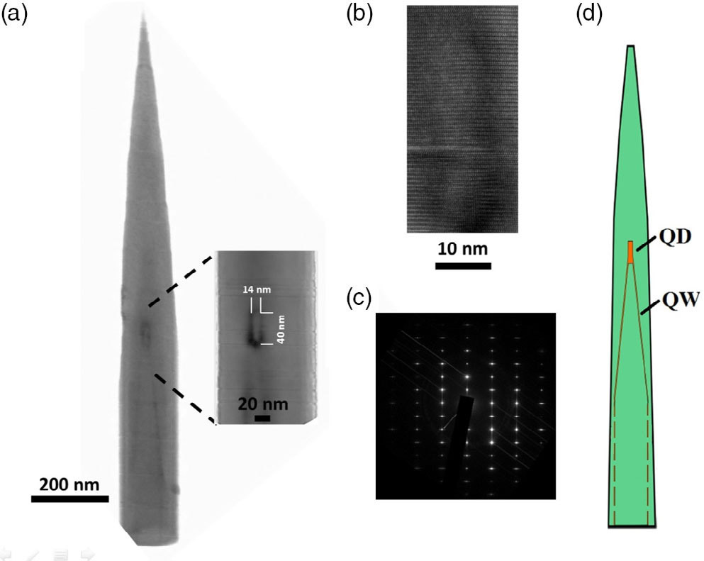
Figure 1: a) Typical transmission electron microscope (TEM) image of single AlGaAs nanowire with InGaAs QD grown at 510°C. b) Typical high-resolution TEM image. c) Typical diffraction pattern obtained at QD location. d) Schematic representation of structure.
The main nanowire material was AlGaAs with ~30% Al content. The InGaAs inclusion was achieved by replacing the Al flow with In after about 20 minutes for about 20 seconds. This resulted in InGaAs QW around the previously grown nanowire and an InGaAs QD tip (Figure 1). Photoluminescence (PL) spectra at low temperature show two prominences associated with the QW and the QD (Figure 2). The QW bump was at shorter wavelength (867nm), indicating higher energy and greater confinement than the QD transitions (1028nm). The room-temperature peak intensity was around 1090nm.
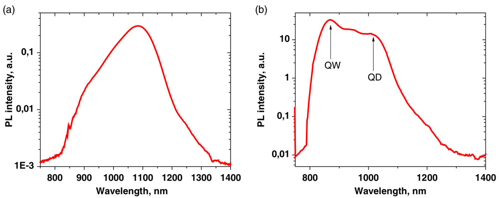
Figure 2: Typical photoluminescence spectra of InGaAs QDs in AlGaAs nanowires grown on silicon measured: (a) at room temperature; (b) at 77K.
The InGaAs material of the QD/QW regions was found to have around 22% In content, according to energy-dispersive x-ray (EDX) analysis. The QD dimensions were 14nm diameter and 40nm height. The QW layer was 2nm thick. The nanowires were typically 1.6μm high with a base diameter of 140nm tapering to 30nm at the tip. The density of nanowires on the silicon substrate was 8x10⁸/cm2.
In-situ reflection high-energy electron diffraction (RHEED) indicated that the main crystal phase of the nanowires was wurtzite, except during the first minute of growth. The fraction of cubic phase was not more than 0.1, according to the diffraction patterns.
The optimal growth temperature was found to be 510°C. Higher temperatures resulted in nanowires that did not produce detectable radiation in the target 800-1300nm wavelength range. The team comments: “In this case, the InGaAs QDs growth process was apparently suppressed due to intensive desorption of In adatoms, leading to the formation of pure GaAs insertion and significant shift of PL band maximum toward ≈800nm.”
On the other hand, reducing the growth temperature to 430°C decreased the integrated luminescence intensity by a factor of 15. The reseachers suggest that this could be either due to increased In content in the QDs with greater lattice mismatch or due to a decrease in the overall quality of the nanowires. Lower growth temperature also resulted in shorter, more tapered nanowires.
MBE InGaAs InGaAs QDs/QWs AlGaAs AlGaAs nanowires
https://doi.org/10.1002/pssr.202200056
The author Mike Cooke is a freelance technology journalist who has worked in the semiconductor and advanced technology sectors since 1997.


