


News: Optoelectronics
24 November 2022
Kyocera develops smallest GaN laser chip mass produced from silicon substrate
Kyocera Corp of Kyoto, Japan has developed a new thin-film process technology for making unique silicon substrates for gallium nitride (GaN)-based micro-light sources (with a side measuring less than 100μm), including short-cavity lasers and micro-LEDs.
Because they offer key performance advantages such as higher definition, smaller size and lighter weight, micro-light sources are considered to be essential to next-generation automotive displays, wearable smart glasses, communication equipment, and medical devices. TrendForce forecasts that the market for micro-LED chips alone will rise at a compounded annual growth rate (CAGR) of about 241% to $2.7bn by 2026.
Technical challenges in making micro-light sources
GaN-based light-source devices, both micro-LED and laser, have typically been fabricated on sapphire and GaN substrates. Conventional processes involve forming a thin GaN device layer for the light source directly onto the sapphire substrate by heating it to a high temperature (1000°C or more) in a controlled gas atmosphere. The device layer has to be then removed (peeled) from the substrate to create a GaN-based micro-light source device. Despite rising demand for smaller devices, however, three separate challenges threaten the ability of this process to achieve miniaturization targets in the near future:
- Difficulty in peeling the device layer
In case of micro-LEDs, existing processes require difficult steps to divide the device layer into individual light sources on the substrate; and then, to separate the device layer from the substrate. As devices become smaller, the technical challenge of this peeling process can result in unacceptably low yield. - High defect density, inconsistent quality
Fabrication of micro-light sources is also problematic because device layers must be deposited onto sapphire, silicon, or other materials with crystal structures that differ from that of the device layer. This creates high defect density and inherent quality-control challenges. - High manufacturing costs
GaN and sapphire substrates are very expensive. Although silicon substrates cost less than sapphire, separating the device layer from a silicon substrate is extremely difficult.
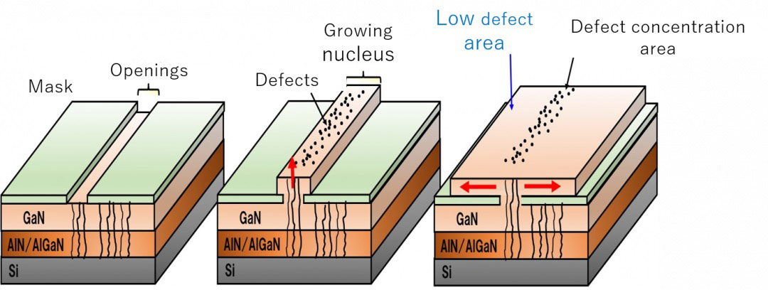
New process developed by Kyocera
Kyocera has developed the new process technology at its Research Institute for Advanced Materials and Devices in Kyoto. First, it grows a GaN layer on silicon substrate, which is available in high volumes at a low cost. The GaN layer is then masked with a non-growing material that features an opening in the center. After this, when a GaN layer is formed on the silicon substrate, GaN nuclei grow over the opening in the mask. The GaN layer, which is a growing nucleus, has many defects at the initial stage of growth; but, by forming the GaN layer laterally, high-quality GaN layers with low defect density can be created, and devices can be fabricated successfully from this low-defect region of the GaN layer.
Kyocera lists advantages of the new process as:
- Easier peeling of the GaN device layer
Masking the GaN layer with a material that does not grow suppresses bonding between the Si substrate and the GaN layer, greatly simplifying the peeling process. - High-quality GaN device layers with low defect density
Since Kyocera’s process can deposit low-defect GaN over a wider area than before, consistent fabrication of high-quality device layers is possible. - Lower manufacturing costs
Kyocera’s new method facilitates successful and reliable separation of the GaN device layer from the relatively inexpensive Si substrate, which will greatly reduce manufacturing costs.
Applications of micro-light sources are listed as:
- Next-generation automotive transparent displays
In the future, the advent of autonomous driving will create demand for displays that are brighter, higher-definition, power-efficient, more highly transparent, and lower cost. - Micro-light sources for AR/VR
The market for micro-light sources used in augmented reality (AR) and virtual reality (VR) is expected to expand rapidly. Smart glasses and other products are being developed to facilitate the creation of virtual spaces through the metaverse in VR and ‘de-smartphoning’ in AR. While conventional semiconductor lasers for AR have been miniaturized to as small as 300μm in length, Kyocera says that it is first to achieve a size of just 100μm. This was achieved by developing a completely new production process that is an evolution of the cleaving method, says the firm. This so’novel cleaving method’ results in a size reduction of about 67% and helps to minimize power consumption. Semiconductor lasers with lower power consumption make it possible to reduce the size and weight of the battery, thus improving fit.
Kyocera says that it will offer a wide range of platform, substrate and process technologies to bring high-quality, low-cost micro-light sources to market in the near future, as it aims to transform next-generation display and laser markets using the new platform.


