


News: Optoelectronics
24 November 2022
Continuous-wave InGaN microdisk laser diodes on (100)-oriented silicon
Suzhou Institute of Nano-Tech and Nano-Bionics (SINANO) in China has achieved room-temperature continuous-wave (CW) current-injected lasing from an indium gallium nitride (InGaN) microdisk laser on standard (100)-oriented silicon (Si) wafers [Meixin Feng et al, ACS Photonics, published online 28 October 2022.
Si(100) substrates are the mainstream basis for complementary metal-oxide-semiconductor (CMOS) integrated circuits. Unfortunately, GaN-based structures are generally grown on Si(111) due to lattice-matching and thermal-expansion constraints. GaN grown on Si(100) suffers from very high threading dislocation (TD) density such that the internal quantum efficiency is much too low for microdisk lasing. Indeed, the SINANO material was first grown on Si(111) and then transferred and bonded to Si(100). At the same time, the team worked on designing a structure that improved thermal management to enhance performance and efficiency.
The SINANO team see their work as potentially leading to efficient on-chip laser sources powering photonics based on GaN waveguides on a low-cost silicon platform. The researchers see further opportunities for quantum optics in areas such as parametric down-conversion, single-photon sources, ion trapping, and cavity quantum electrodynamics, along with biosensing and visible light communication.
The laser structure (Figure 1) was first grown p-side up, allowing proper activation of the p-type magnesium-doped layers before wafer bonding. Activation involves thermal annealing to drive out hydrogen from the growth process, which passivates the magnesium acceptors. The laser material was then flip-wafer bonded to the Si(100) substrate, and the metal-organic chemical vapor deposition (MOCVD) Si(111) growth substrate was removed.
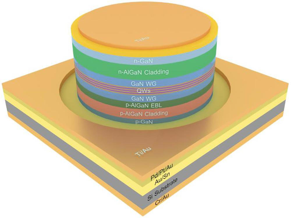
Figure 1: Schematic diagram of p-side down GaN-on-Si(100) microdisk laser.
The growth template consisted of aluminium nitride (AlN) seed layer, followed by two AlGaN stress-control and defect (e.g. TD) reduction layers, before application of the 2.6μm n-GaN template layer itself. The laser structure included three 2.5nm indium gallium nitride (In0.12Ga0.88N) quantum wells separated by 12.5nm In0.02Ga0.98N barriers. The waveguide layers were GaN: 90nm on the p-side and 140nm n-side. The cladding consisted of doped AlGaN, 600nm p-side (7% Al) and 500nm n-side (8% Al). An AlGaN electron-blocking layer (EBL) was 20nm thick. In the fabricated device, the n- and p-side contact layers were 30nm and 50nm, respectively.
The Si(100) wafer was bonded to a palladium/platinum/gold (Pd/Pt/Au) p-electrode of the laser structure with gold-tin (AuSn). After bonding the growth substrate and template layers were removed, using wet etch for the Si(111), and plasma for the AlGaN and for partly thinning the n-GaN. The surface was then subjected to chemical mechanical polishing (CMP), further thinning the n-GaN to the target thickness. The n-electrode consisted of titanium/platinum/gold (Ti/Pt/Au). The microdisks were then sculpted using more plasma etch, before applying the final Ti/Au contact metals.
Since the microdisk etching was critical for reducing surface damage and tilt angle, which affects both non-radiative recombination and reflectivity, the researchers tested six different inductively coupled plasma (ICP) etch recipes. The best used a chlorine/boron trichloride/nitrogen (Cl2/BCl3/N2) mix, which gave the most vertical sidewalls (~87°).
Under CW operation, the device emitted single-mode laser light with a 402.9nm wavelength (Figure 2). The researchers estimated from the 20μm microdisk radius that this corresponded to about the 776th whispering gallery mode. The spectrum and behavior of the full-width at half-maximum (FWHM) suggest that lasing sets in around 60mA injection. Once lasing dominates, above 70mA current, the output power was about 30% less than that of a reference device on Si(111). The researchers comment that, in their setup, “only a small proportion of the optical output power was gathered from the microdisk sidewall.”
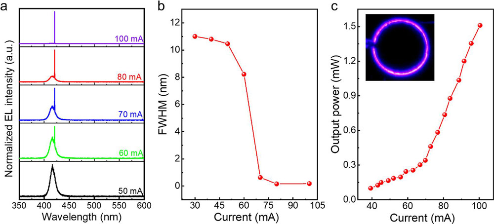
Figure 2: (a) Normalized electroluminescence (EL) spectra and (b) FWHM of 20μm radius GaN-on-Si(100) microdisk laser measured under CW injection currents. (c) Optical output power versus injection current curve. Inset: top-view EL image at 50mA — part of circular emission pattern obstructed by electrical probe.
The operating voltage at 70mA was 4.8V, some 29% lower than for the reference on Si(111). This means that the electrical resistance was much less, giving lower power loss and lower Joule heating, which should reduce thermal degradation effects. The researchers attribute these improvements to the reduction in current-crowding effects, an optimized n-type Ohmic contact, and reduced thickness of the n-AlGaN cladding.
“Reduced operation voltages, together with a lower threshold current, contributed to 50% less injected electrical power for the as-fabricated GaN-on-Si(100) microdisk laser,” the team writes.
By studying the temperature dependence of the forward voltage at 70mA pulsed injection, the researchers estimate the thermal resistance of the microdisk at 95K/W, some 32.5% less than for the reference lasers on Si(111). The team attributes the lower resistance to the thinning of the AlGaN layers, which have low thermal conductivity. Also, in the flip-wafer bonding process the AlGaN stress/defect reduction layers are completely removed from the thermal dissipation path, while these block heat flow in the reference device.
The team comments: “The reduced thermal resistance and less injection electrical power contributes to a 66.5% reduced junction temperature, which means that the as-fabricated 20μm radius GaN-on-Si(100) microdisk laser can operate in CW mode while our previous conventional GaN-on-Si(111) microdisk laser cannot.”
The lifetime of the microdisk laser on Si(100) at 77mA is quoted at “several minutes”. The researchers apportion blame: “The restricted lifetime is primarily related to the relatively high TD density due to a huge mismatch in the thermal expansion coefficient and lattice constant between GaN and Si(111).”
The lifetime could be increased to the order of 10,000 hours if the TD density could be reduced to the 106/cm2 level. The team are looking to improvements such as using freestanding GaN as the growth substrate with appropriate substrate lift-off with a view to recycling the very expensive material relative to silicon.
The author Mike Cooke is a freelance technology journalist who has worked in the semiconductor and advanced technology sectors since 1997.


