


News: LEDs
3 November 2022
Ultra-stable emission from green micro-LEDs on silicon
University of Michigan in the USA reports “for the first time, μLEDs grown directly on silicon with submicron lateral dimensions” [Yuanpeng Wu et al, Light: Science & Applications, v11, p294, 2022]. The resulting indium gallium nitride (InGaN) devices featured ultra-stable green wavelength emission due to reduced quantum-confined Stark effects (QCSEs), which result from strain-dependent electrostatic fields from different charge polarizations of the various chemical bonds.
With the usual GaN barriers between the InGaN multiple quantum wells (MQWs), these QCSEs cause a large blue-shift in the emission wavelength of light-emitting diodes (LEDs) as the applied voltage increases for increased current injection. Such a shift in wavelength is particularly unwanted in full-color display applications. The Michigan devices used aluminium gallium nitride (AlGaN) barriers instead, enabling polarization and strain engineering to reduce QCSE.
The researchers comment: “This work provides a new approach for designing the active region of high-performance multi-color μLEDs.”
The team sees opportunities in on-chip optical communication, and augmented reality/mixed reality (AR/MR) and ultrahigh-resolution full-color displays. Further, the deployment on low-cost silicon (Si) substrates could lead to seamless integration with mainstream CMOS electronics.
The template consisted of an N-polar 500nm n-GaN buffer on 100nm AlN seed grown on 2-inch Si(111) by plasma-assisted molecular beam epitaxy (PAMBE).
The nanowires were grown by bottom-up selective area epitaxy (SAE) using a thin titanium mask (Figure 1). The nanowire growth sequence consisted of ~450nm Si-doped n-GaN, six periods of InGaN/AlGaN multiple QWs (MQWs), and ~170nm Mg-doped p-GaN. The InGaN QWs were 12nm thick. The successive AlGaN barrier layers extended to form AlGaN/GaN superlattice shells around the nanowire QWs. The barrier Al content was about 15%, according to x-ray energy-dispersive spectroscopy (EDS) line scans. The indium content of the wells varied up to around 30%.
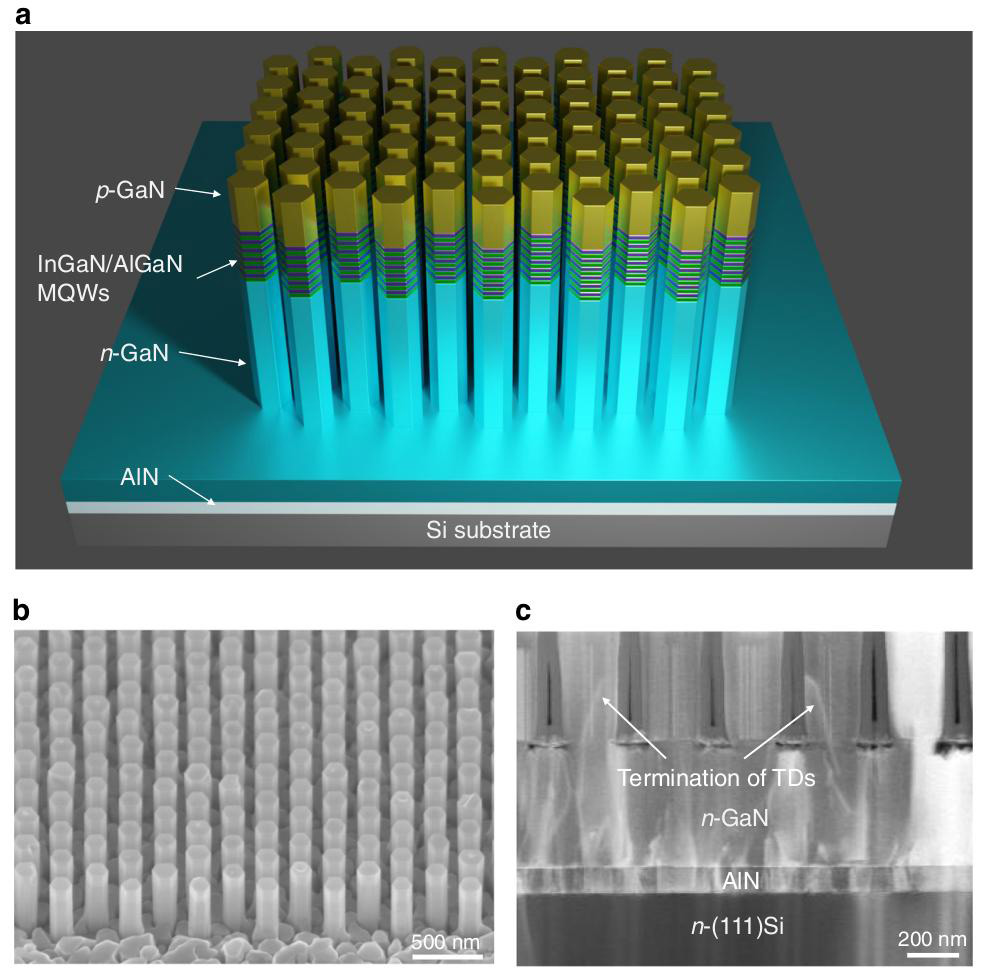
Figure 1: (a) Schematic of InGaN/AlGaN MQWs-in-nanowire heterostructure grown on silicon substrate. (b) Bird’s-eye view scanning electron micrograph (SEM) of as-grown InGaN/AlGaN p-i-n nanowire arrays. (c) Cross-sectional scanning transmission electron micrograph (STEM) of nanowire on silicon substrate, showing termination of TDs on sidewall of n-GaN nanowire before reaching active region.
The hexagonal cross-section of the wires came from the six equivalent m-planes of the GaN wurtzite crystal structure. The tops of the wires were flat, c-plane, unlike metal-polar III-N material that tends to result in pyramid tops.
The nanowires also did a decent job in filtering threading dislocations (TDs), reducing the density by 85% from ~3x10¹⁰/cm2 in the GaN buffer. The filtering was more effective in thinner nanowires, less than 150nm diameter.
Comparison was made with nanowires with GaN barriers. In photoluminescence (PL) experiments, the quantum-confined Stark effect in nanowires with GaN barriers was seen in narrowing of the spectral peak with increase in excitation power. No such narrowing was seen in samples with AlGaN-barrier nanowires. The GaN-barrier wires also showed a significant ~100nm blue-shift in photon wavelength (another signal of QCSE).
The researchers see the reduced QCSE in AlGaN-barrier nanowires as resulting from polarization doping effects in the shell region, creating donor-type surface states and bulk shallow donors. The induced electrons then migrate to the QWs in the nanowire core, screening the electrostatic fields that cause QCSE.
The AlGaN-barrier nanowires had two dominant peaks, which were attributed to different parts of the QW: in the central region the QW grew in the c-plane direction, resulting in polar material producing emissions at 2.36eV photon energy (525nm wavelength); toward the edge, however, the material became semi-polar, emitting at lower energy and longer wavelength (2.23eV/556nm).
Another effect of the AlGaN barrier was pseudomorphic growth, with the tensile strain of the InGaN layers being compensated by the smaller lattice constant of AlGaN relative to GaN. The smaller mismatch strain energy is expected to result in enhanced indium content in the QWs, giving longer-wavelength emissions, and significantly reduced strain relaxation.
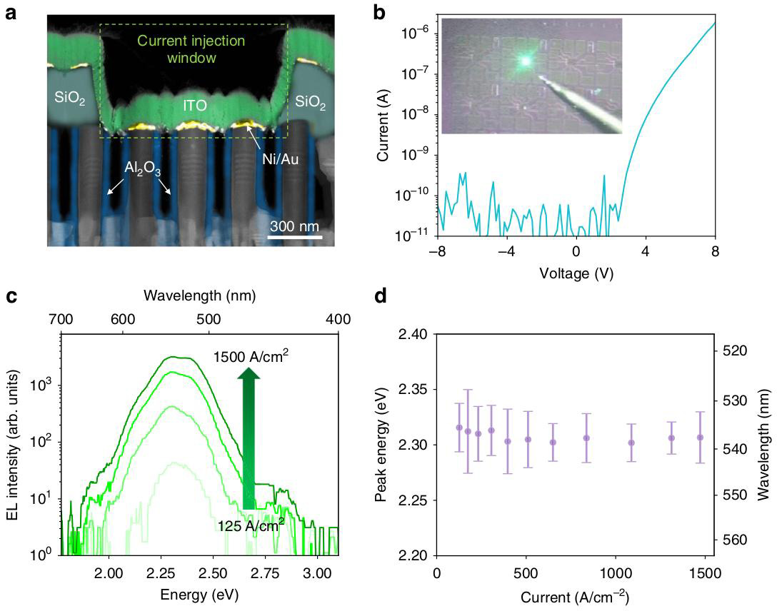
Figure 2: (a) Cross-sectional high-angle annular dark-field (HAADF)-STEM false-color image of as-fabricated InGaN/AlGaN μLED (blue: Al2O3; dark-cyan: SiO2; yellow: Ni/Au; green: ITO). (b) Current-voltage characteristics at room temperature. Inset: Optical image of bright green emission under injection current of ~100A/cm2. (c) Electroluminescence spectra. (d) Variation of peak position versus injection current.
The researchers fabricated the material into μLEDs of 900nmx900nm area (Figure 2). The sidewalls were passivated with atomic layer deposition (ALD) aluminium oxide (Al2O3) against leakage currents from short-circuiting caused by subsequent metal deposition. The p-GaN tops of the nanowires were passivated/insulated with 320nm plasma-enhanced chemical vapor deposition (PECVD) silicon dioxide (SiO2). The emission window/transparent conductor contact with the p-GaN was formed by annealed 2.5/2.5/180nm nickel/gold/indium tin oxide (Ni/Au/ITO). The n-contact was titanium/gold.
The devices demonstrated negligible leakage current at reverse bias with a rectification ratio of four orders of magnitude at ±8V. The diode turn-on came at ~3V. The dominant peak emission was ~2.3eV (537nm), which was barely affected by increasing current.
A red-shift from ~2.313eV (536nm) to 2.309eV (537nm) with increasing current is described as “slight”. The researchers comment: “This is in direct contrast with previously reported green-emitting InGaN QW LEDs, wherein a blue-shift of 20–50nm due to QCSE and color instability were widely observed.” The tiny red-shift observed in the Michigan devices is put down to “a combination of the current-induced heating effect and bandgap renormalization,” by the team.
The researchers also suggest that their structure could suppress the impact of Auger recombination due to reduced carrier density within the InGaN QWs, resulting in less efficiency droop with increased current, compared with conventional devices.
The author Mike Cooke is a freelance technology journalist who has worked in the semiconductor and advanced technology sectors since 1997.


