


News: LEDs
12 October 2022
Multi-wavelength emission from 3D structured InGaN
Kyoto University in Japan has demonstrated a 90nm wavelength spread for the light emission from indium gallium nitride (InGaN) quantum well (QW) structures grown on convex-microlens structured GaN templates on sapphire [Yoshinobu Matsuda et al, Appl. Phys. Express, v15, p105503, 2022]. The researchers mainly attribute the spread to differing indium incorporation as the off-angle from planar deposition varied.
The team comments: “We believe that the gently sloping 3D structures will facilitate future LED device processing. In addition, the continuously changing off-angle of the microlens shape provides the continuously changing emission wavelength. Therefore, we expect that the desired wavelength components can be extracted by electrically accessing the corresponding local position.”
The researchers hope their work could contribute to achieving white light-emitting diodes (LEDs) without phosphors, high-capacity communications by wavelength division multiplexing in LiFi systems, and spontaneously arrayed micro RGB LEDs for display applications.
The researchers used thermal reflow to form GaN microlens-shaped bumps on the surface on GaN/sapphire templates (Figure 1). The microlenses were defined by photoresist disks and lithography that were transformed into convex lens shapes by heating on a hotplate at 180°C for 40 minutes. The shaping was then transferred from the photoresist to the underlying GaN by inductively coupled plasma reactive ion etch (ICP-RIE). The device layers were applied by metal-organic vapor phase epitaxy (MOVPE): 500nm 1050°C undoped GaN (u-GaN), followed by a single 2.5nm/11nm 700°C InGaN/GaN quantum well.
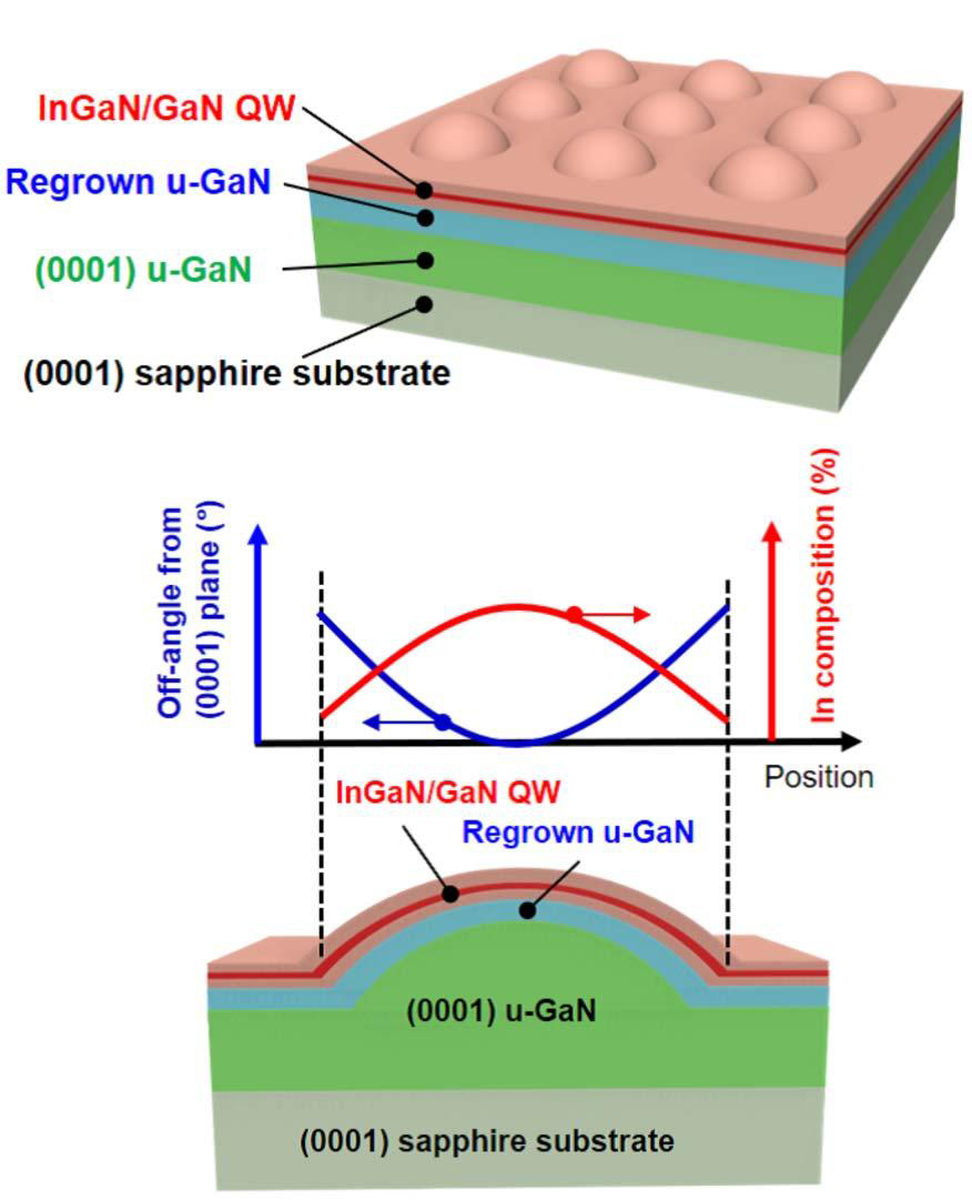
Figure 1: (Top) Material structure grown on microlens array on (0001) GaN/sapphire template and (bottom) cross-sectional view of single microlens, with sketch graph showing off-angle variation and expected indium composition distribution.
The convex lens shape was maintained up to 30μm diameter. Beyond that, the structures tended to exhibit a concave dip in the middle. Such dips also showed up when the reflow temperature or time were reduced in smaller-diameter structures. The QW layers reduced the maximum off-angle from 11° to 8° in samples with 20μm-diameter microlenses. The microlens heights were ~1.5μm before and after MOVPE, but the lateral diameter increased from 20μm to 50μm. The researchers suggest that “the surface adatoms diffuse from the top of the microstructure or the planar region around the microstructure to the bottom.”
The variation of indium incorporation across the microlens structure was evaluated using cathodoluminescence (CL) at various positions (Figure 2). The peak wavelength varied across the microlens from 490nm down at the center to 400nm near the edge. The total emission with a peak at 410nm was dominated by the shorter wavelengths due to the lower indium incorporation and larger area of the circumference relative to the regions towards the center. Higher-indium-content InGaN tends to have lower emission efficiency.
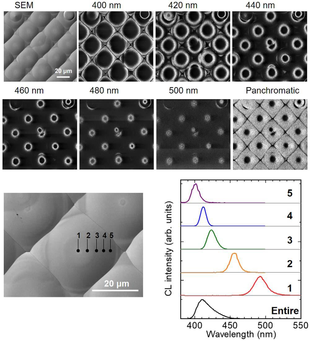
Figure 2: (Top) Scanning electron microscope (SEM) image of InGaN QWs on GaN microlens structures and monochromatic CL mapping images taken at various wavelengths. (Bottom) Spatially resolved CL spectra (right) at given positions of microlens (left) and across entire structure.
The wavelength spread of 90nm is wider than previously reported work by the Polish Institute of High Pressure Physics which showed a 40nm spread with the off-angle varying up to 2.4°. The off-angle profile of the Kyoto microlens structures reached around 8°. From other research, it is thought that, while off-angles in the low range exhibit reduced indium incorporation with increasing off-angle near zero, beyond about 30° the indium incorporation increases up to a maximum at 60°.
Another possible effect affecting the peak wavelength could be the effective width of the QW, which naturally varied through the microlens profile. However, on the basis of transmission electron microscope and energy-dispersive x-ray studies, the researchers conclude the dominant factor determining indium composition was the off-angle dependence of indium incorporation, modified by the surface diffusion of gallium atoms during the MOVPE process.
The author Mike Cooke is a freelance technology journalist who has worked in the semiconductor and advanced technology sectors since 1997.


