


News: Optoelectronics
27 October 2022
Pocketing benefits for QD lasers on 300mm silicon
University of California Santa Barbara, USA, reports “the first electrically pumped in-pocket Fabry–Perot quantum dot lasers grown by MBE emitting around 1300nm with cleaved facets, sustaining lasing characteristics up to 60°C with a wall-plug efficiency of 8.6%” [Chen Shang et al, Light: Science & Applications v11,p 299, 2022]. The team also included researchers from IQE Inc and RF SUNY Polytechnic Institute in the USA and NAsPIII/V GmbH in Germany.
It is hoped that the in-pocket laser diodes (LDs) will be easier to integrate into silicon (Si) and silicon-on-insulator (SOI) photonic structures than light-emitting devices applied by wafer bonding or direct epitaxial growth using blanket deposition techniques. In particular, in-pocket lasers can be butt-coupled on a level with silicon nitride (SiN) or SOI waveguide cores, rather than evanescent coupling, which is used with wafer bonding, and difficult to achieve with epitaxial structures with the light-absorbing thick buffer layers needed to reduce defect formation and propagation into the device layers. The use of an indium arsenide (InAs) quantum dot (QD) active region also promises to be less affected by any defects that remain.
The team comments: “With additional lithography and etching steps and/or alternative layout designs, a variety of active components such as semiconductor optical amplifiers, mode-locked lasers, or distributed-feedback lasers can also be fabricated from the same chip. This fabrication process can be used in integrating complex photonic circuits on 300mm-diameter SOI wafers.”
The pocket LDs were fabricated on a 300mm silicon photonic template with tetraethoxysilane (TEOS) oxide patterning (Figure 1).
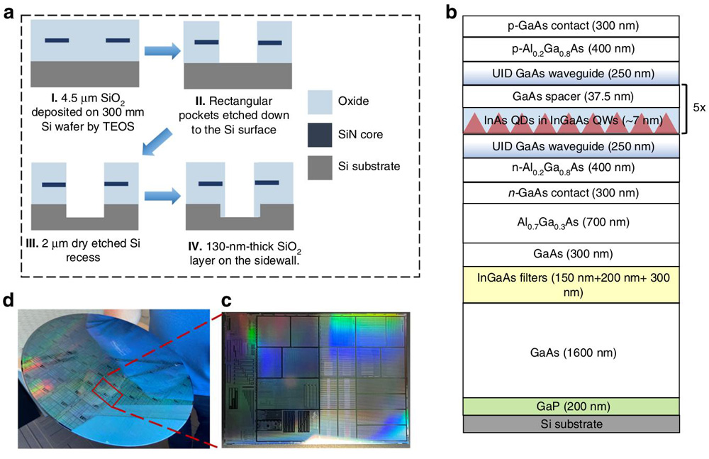
Figure 1: (a) Pattern formation process before III–V deposition. (b) Simplified III–V laser stack. (c) Diced coupon from as-patterned 300mm silicon wafer for growth condition investigation. (d) As-patterned 300mm silicon wafer.
One challenge of the pocket structure was to obtain suitable temperature control in the molecular beam epitaxy (MBE) used for the device layers. This was critical due to the very narrow window (±2.5°C) for the InAs QD nucleation in the indium gallium arsenide (InGaAs) multiple quantum well (MQW) layers. Unfortunately, unlike in blanket MBE, reflective high-energy electron diffraction (RHEED) in-situ monitoring of the growth process was not possible due to interfering signals from the non-pocket regions, so the researchers had to depend on pyrometer readings calibrated from separate experiments on diced coupons of material.
It was found that the temperature in the pocket regions were possibly 45°C higher than the non-pocket regions. The higher temperature evaporated indium from the growth front, inhibiting QD formation.
Further work showed that a 30°C reduction in growth temperature was needed for QD formation with a ground-state photoluminescence peak around 1300nm wavelength. The full width at half maximum was 32meV, and the ground-to-excited-state peak separation 70meV; “comparable to typical values for blanket silicon substrates,” the team adds.
Growth of the structure on a 300mm wafer was then carried out using the derived conditions. The seed layers of 200nm gallium phosphide (GaP) and 500nm GaAs were applied at NAsPIII/V, using metal-organic chemical vapor deposition (MOCVD). The devices layers were applied at IQE by MBE.
The wafer was diced into rectangular coupons for fabrication into laser diodes at UCSB’s Nanofab (Figure 2). The QD laser fabrication was eased by the previous removal of polycrystalline residue from the growth process by wet etch and planarization. The team comments: “The removal of surface polycrystal enables easier handling with a more planarized sample surface and better focus calibration in the photolithography steps.”
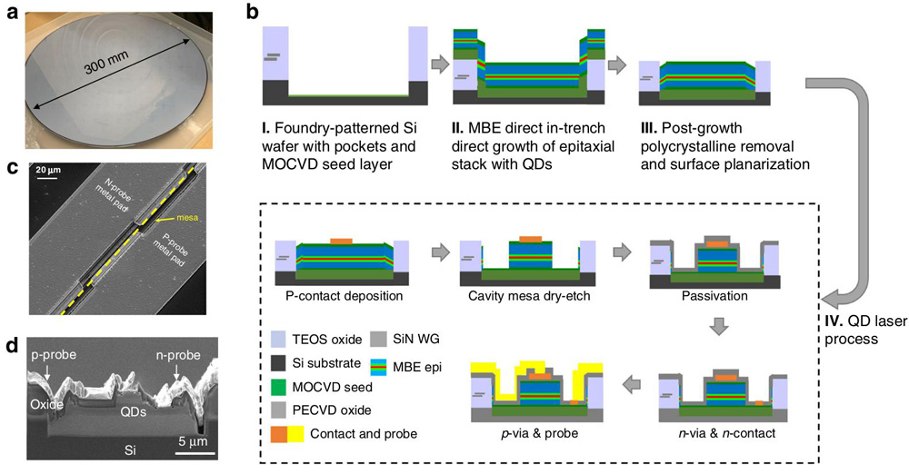
Figure 2: (a) As-grown 300mm wafer from IQE, covered with polycrystalline III–V material. (b) Simplified fabrication flow for laser fabrication, not drawn to scale. (c) Top-down view of as-fabricated device. (d) Cross-section scanning electron micrograph (SEM) of as-cleaved in-pocket laser.
The resulting laser diodes had a ridge waveguide of 3.5μm width in a 20μm-width pocket. The maximum double-sided laser output power was 126.6mW continuous wave (CW) at 20°C. The laser threshold was at 47.5mA. The researchers say that the performance is comparable to devices grown on blanket silicon substrate with similar threading dislocation density (TDD). The maximum double-sided wall-plug efficiency was 8.6% at 214mA. CW lasing continued up to 60°C, and pulsed lasing to 70°C.
The researchers hope that thermal management concerns of the pocket structure can be overcome through template quality, growth condition, device design, and other optimizations. Aging experiments showed about a 10% increase in bias current needed for 10mW output power after 350 hours, comparable to devices on blanket silicon.
Laser diodes 1300nm laser diodes InGaN MBE GaP GaAs MOCVD
https://doi.org/10.1038/s41377-022-00982-7
https://sunypoly.edu/sponsored-research/research-foundation.html
The author Mike Cooke is a freelance technology journalist who has worked in the semiconductor and advanced technology sectors since 1997.


