


News: Microelectronics
20 October 2022
RF detection with InGaAs and GaN HEMTs
Researchers based in Spain and France report on the relative merits of indium gallium arsenide (InGaAs) and gallium nitride (GaN) high-electron-mobility transistors (HEMTs) as radio frequency (RF) signal detectors [G. Paz-Martínez et al, J. Appl. Phys., v132, p134501, 2022].
The researchers — six from Universidad de Salamanca, Spain, and one from Université de Lille/Université de Valenciennes, France — believe that the InGaAs HEMT RF detection frequency range could reach at least the sub-terahertz range and perhaps even above 1THz.
The devices were operated in the region of “third-quadrant conduction” (TQC) where a sharp non-linear increase in drain current occurs due to the channel opening for negative values of drain bias.
The researchers compared the RF detection performance of HEMTs with aluminium gallium nitride (AlGaN) and indium aluminium arsenide (InAlAs) barrier material (Figure 1). The GaN/InGaAs HEMT materials had Hall sheet electron densities of 1.3x10¹³/cm2 and 1.5x10¹³/cm2 with mobilities of 1800 and 3400cm2/V-s at 300K, respectively.
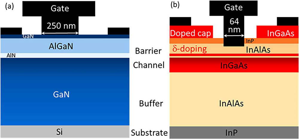
Figure 1: Sketch of (a) GaN and (b) InGaAs HEMTs.
The gate electrodes had two fingers of 2x25μm width in the GaN device, and 2x35μm for the InGaAs HEMT (Figure 2). The higher-mobility, wider InGaAs device had a lower open-channel resistance (Ron) of 32Ω compared with the GaN HEMT’s 66Ω. The researchers comment: “This parameter will play an important role in the RF detection performances of the devices since it will strongly affect the input mismatch with the 50Ω RF source.” To facilitate RF probing, the devices were fabricated with coplanar waveguide accesses.
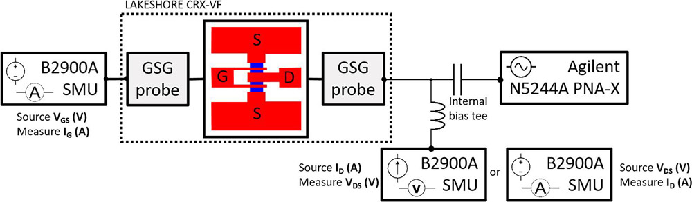
Figure 2: Schematic drawing of DC and RF characterization setup for drain terminal injection.
The samples were probed with ground-source-ground (GSG) probes in a CRX-VF cryogenic probe station. The RF source was a PNA-X vector network analyzer (VNA). Two-channel source-measurement units (SMUs) were used to bias the drain and gate terminals of the transistors. Coupling of the AC and DC signals was through an internal bias-tee.
The devices were tested under a 1GHz RF signal with input powers of -15dBm and -31dBm for the GaN and InGaAs HEMTs, respectively. The researchers comment: “These values correspond to the actual power delivered to the device since the output power of the VNA has been increased to compensate losses due to the cables, connectors, and probes.”
The transistors were operated with quiescent bias point (Q-point) in zero drain current(ZC)/open- and zero drain-source voltage(ZV)/short-circuit modes to provide voltage and current responsivities, respectively, to input power from a 50Ω impedance supply, as typical from coax cables with balanced power handling and insertion loss. In the ZC mode the researchers measured the shift in drain-source voltage (VDS). The ZV mode had the team looking for a shift in drain current (IDS).
The results (Figure 3) showed that a quasi-static (QS) model, previously developed by the team, based on non-linearity of the DC current-voltage behavior, along with dependencies on the values of the drain conductance (gD) and its bowing coefficient (γ=∂(log(gD)/∂VDS), gave a reasonable fit to the various performances.
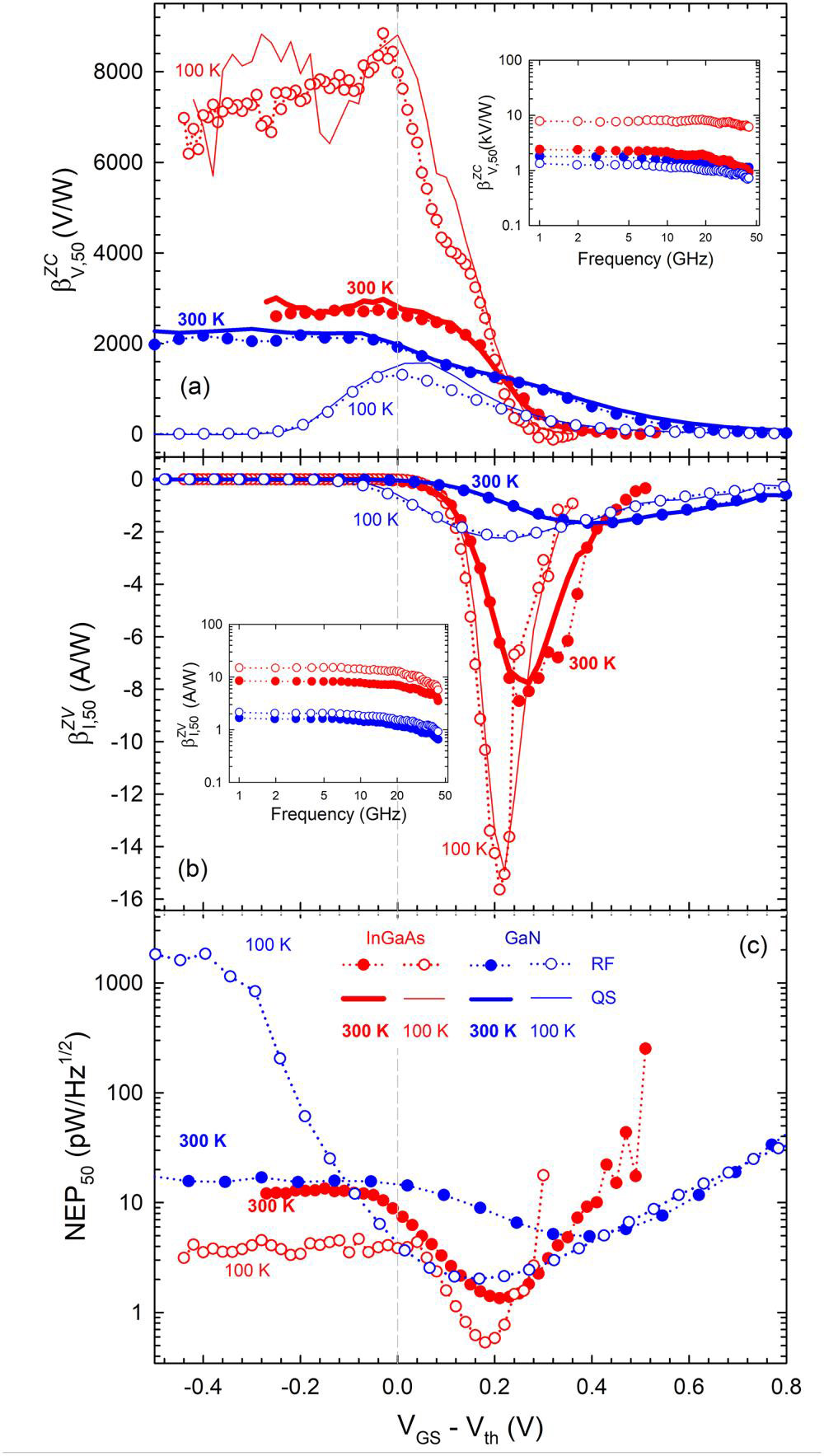
Figure 3: Comparison of the QS values and experimental measurements with 50Ω input signals of (a) ZC and (b) ZV responsivities (βZCV,50 and βZVI,50, respectively) at 300K and 100K. Insets show frequency dependence of measurements at VGS bias providing maximum responsivities. (c) Noise equivalent power (NEP50) extracted from ZC measurements compared with QS-model.
The InGaAs device gave significantly better performance for RF detection at room (300K) and cryogenic (100K) temperatures. The failure of the GaN HEMT to give enhanced performance in a cryogenic environment was related to the lack of a back barrier provided in the InGaAs device by the double-heterostructure quantum well channel. The GaN device therefore suffered from buffer leakage and hence inadequate pinch-off.
The team explains: “Concerning the RF detection performances, InGaAs HEMTs provide much higher responsivity and lower noise equivalent power (NEP) due to the enhanced non-linearity of the gD, evidenced by a much larger value of the γ coefficient. This is closely linked to the better gate-channel control offered by this technology which, due to its higher mobility, intrinsically provides a superior transconductance level as compared to GaN HEMTs.”
The researchers also investigated the ability to improve impedance matching of the InGaAs device by also studying devices with 2x15μm and 2x25μm widths. The team’s QS model also adequately represented the performance, allowing the researchers to speculate on how to achieve perfect matching. Ideally the width would have to be increased, maybe up to 2mm for a low gate-source bias (VGS). With a relatively high VGS of -0.35V, the width would need to fall in the range 200-400μm for current-mode detection.
The author Mike Cooke is a freelance technology journalist who has worked in the semiconductor and advanced technology sectors since 1997.


