


News: Optoelectronics
1 September 2022
Room-temperature CW InGaAs 980nm laser diodes on on-axis silicon
China’s Beijing University of Posts and Telecommunications has demonstrated room-temperature continuous wave (RT-CW) operation of 980nm indium gallium arsenide (InGaAs) quantum well (QW) laser diodes (LDs) directly grown on on-axis silicon (Si) (001) [Chen Jiang et al, Appl. Phys. Lett., v121, p061102, 2022].
The team comments: “RT-CW operation of silicon-based GaAs-buffered III–V QW lasers directly grown on on-axis Si (001) substrates has not been realized until now.”
It is hoped that such directly integrated devices could reduce the costs of optoelectronic integrated circuits (OEICs) fabricated on silicon platforms through eased mass production, compared with using external light sources or wafer bonding of III-V light emitters.
Barriers to heteroepitaxy of III-V materials on silicon include crystal defects such as threading dislocations (TDs), antiphase domains (APDs), and micro-cracks. These defects tend to seriously reduce the optoelectronic performance of III-V structures.
One way to reduce the impact of TDs on performance is to use quantum dots rather than QWs. However, the implementation of QWs on silicon is attractive since it would allow the transfer of the vast engineering knowledge from commercial light-emitting devices grown on III-V substrates to the silicon platform.
The 420nm GaAs template (Figure 1) was grown by metal-organic chemical vapor deposition (MOCVD) on on-axis Si (001). The precursors were trimethyl-gallium and arsine (AsH3). The silicon substrate was subjected to an annealing treatment in hydrogen to avoid anti-phase domain formation.
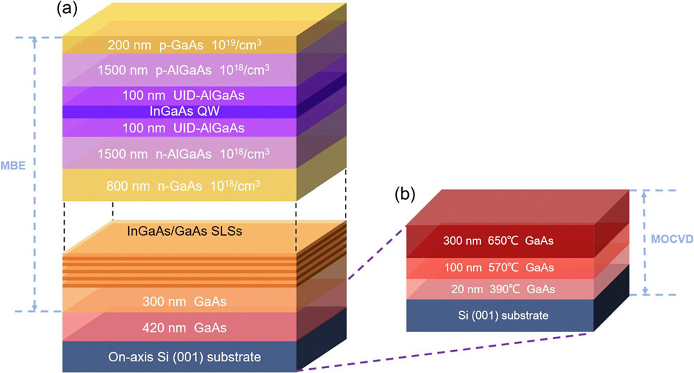
Figure 1: (a) Schematic of QW laser directly grown on on-axis Si (001). (b) MOCVD scheme for initial 420nm GaAs/Si (001) template layers.
The remainder of the device was grown using solid-source molecular beam epitaxy (MBE). The template had a root-mean-square roughness of 0.91nm. The first 300nm GaAs buffer layer flattened the growth surface further. Rough surfaces have been found to lead to non-radiative recombination via exciton generation, sapping laser performance. Four sets of 5x(10nm/10nm) strained-layer superlattices (SLSs) separated by 300nm GaAs spacers filtered out dislocations. The threading dislocation density (TDD) at the n-GaAs contact surface was 4.9x10⁷/cm3.
The active 8nm InGaAs QW was embedded in an unintentionally doped (UID) aluminium gallium arsenide (AlGaAs) waveguide structure of two 100nm layers. The doped cladding layers were 1500nm. The bottom n-contact was 800nm; the top p-contact was 200nm. The n- and p-type doping were supplied by silicon (Si) and beryllium (Be), respectively. The laser layers were grown in an As2 atmosphere.
A reference structure was also produced on a GaAs substrate.
The material was fabricated into stripe Fabry-Pérot laser diodes with 21.6μm x 1mm cavities. The mirror end facets were formed by wafer cleaving without any optical coatings being applied. The laser diode chips were mounted on copper heatsink in C-mount packages. The measurements were carried out at room temperature (25°C).
In 5% duty-cycle 50μs pulse operation the laser threshold current density was 328A/cm2 (70.5mA) for the device on GaAs substrate (Figure 2). For the silicon substrate laser diode the density was more than twice that at 768A/cm2 (165.1mA). While one wants the threshold to approach that of GaAs-based devices, the team points out that all previous reports of InGaAs laser diodes on on-axis Si (001) have had higher thresholds still.
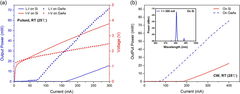
Figure 2: Room-temperature performance of laser diodes on GaAs and Si substrates in (a) pulsed and (b) CW operation at room temperature. Inset: lasing spectrum of Si-based laser at 300mA.
The slope efficiency of the laser diode on silicon was 0.113W/A, and the single-facet output power 15.5mW at 300mA. The power at that point showed no sign of attenuation, according to the team.
The threshold current density increased in CW operation to 381A/cm2 (81.9mA) and 867A/cm2 (186.4mA) for the GaAs- and Si-based laser diodes, respectively. The corresponding output powers at 400mA were 75.6mW and 22.5mW. The slope efficiencies were 0.24W/A on GaAs substrate, and 0.097W/A on silicon.
The researchers attribute the poorer performance under CW operation to thermal effects from heat accumulation, which is avoided in pulsed mode. Lower thresholds on silicon have been achieved on misoriented Si (331A/cm2), but on-axis Si is preferred in the context of integration with mainstream silicon electronics.
CW operation of Si-based laser diodes at 300mA injection resulted in a laser peak at 980.8nm wavelength. The lifetime of the initial devices was 90s, but the team was able to optimise the devices to give a longer 12 minute life at 23°C.
The team admits that there is “a long way to go to make the lifetime of these lasers comparable to that of the currently demonstrated Si-based QD lasers”, adding: “The essential issue to fulfil this target should be dramatically further reducing the TDD of the heteroepitaxial GaAs virtual substrate.”


