


News: Optoelectronics
5 September 2022
GaNo Opto launches first silicon carbide EUV photodiode
GaNo Optoelectronics Inc – a spin-off from China’s Nanjing University that offers ultraviolet (UV) detectors and modules based on wide-bandgap semiconductors including gallium nitride (GaN) and silicon carbide (SiC) – has formally released what it claims are the first commercial SiC-based extreme ultraviolet (EUV) photodiodes.
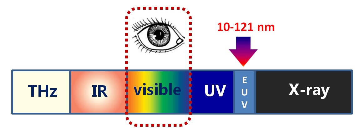
Figure 1: Distribution of optical emission spectrum from THz to x-ray.
With the rapid development of VLSI fabrication technologies down to 7/5nm nodes (for micro-chips containing billions of transistors), advanced photolithography is transitioning from deep ultraviolet (DUV) immersion lithography based on a 193nm light source to extreme ultraviolet (EUV) lithography based on 13.5nm light source. An EUV lithography system is so complex that demanding technical challenges must be overcome for meeting chipmakers’ requirements for high-volume manufacturing. Among them, the development of high-performance EUV detectors is critical because, to precisely control the photoresist exposure dose, the intensity and uniformity of the EUV light beam must be constantly monitored. Besides EUV lithography, semiconductor EUV detectors are also core components in solar-observing satellites, materials science and many fundamental research fields.
Traditionally, commercial EUV detectors are solely based on silicon (Si), which have been demonstrated with certain success but suffer from several intrinsic drawbacks. For example, although silicon EUV detectors could exhibit moderate quantum efficiency in the EUV wavelength range, they require highly complex optical filters to achieve a high UV/visible rejection ratio as their peak response stays within the visible wavelength range. In addition, silicon detectors are not suitable for working in harsh environments, which would degrade considerably upon high-fluence EUV irradiation.
“It has been well accepted that wide-bandgap semiconductor is the most suitable material for making UV photodetectors,” says chief technology officer Dr Hai Lu, who is also distinguished professor at Nanjing University. “Due to the wide-bandgap nature of SiC, EUV photodiodes based on SiC have no response to background white light and could exhibit very low dark current down to 1pA even at a high temperature of 150℃. This means that the SiC EUV photodiodes have extremely low noise, leading to very high signal-to-noise ratio and detectivity. Meanwhile, it has been confirmed that the radiation hardness of SiC photodiodes is at least 1000 times higher than their silicon counterparts, due to the high electron-hole pair ionization energy and displacement threshold energy of SiC semiconductor,” he adds.
GaNo Opto says that its new intrinsically visible-blind EUV photodiodes can work in either photovoltaic or photoconductive mode with high EUV photon detection efficiency, high response speed and high stability.
Despite the apparent advantages, the implementation of SiC EUV photodiodes is very challenging due to substrate- or epi-related material defects, relatively poorly modeled device operation, and immature device processing technology. “Our process shows that appropriate surface electric field modulation and surface passivation techniques are critical for realizing SiC EUV photodiodes with low leakage current and long-term stability, both of which are necessary for high-end applications in advanced lithography systems or space satellites,” Lu says.
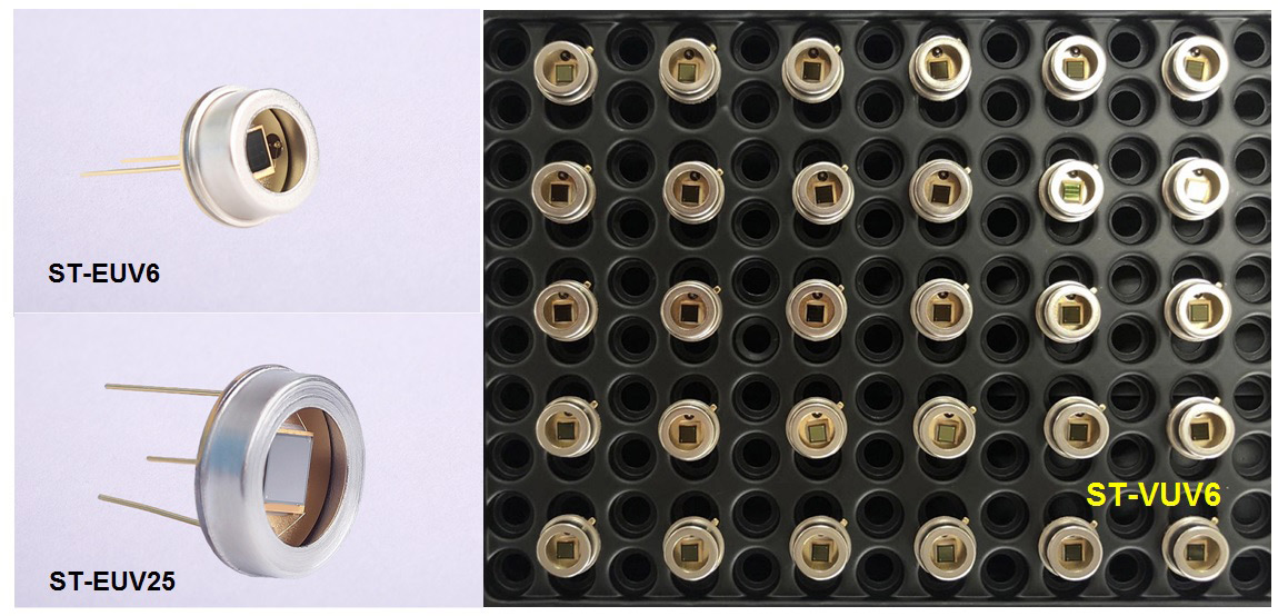
Figure 2: Some of GaNo Opto’s newly released EUV and vacuum UV detectors.
After pilot production and multiple customer verifications beginning from October 2021, GaNo Opto has started to ship SiC EUV photodiodes and components to several major customers worldwide.
“Our next step is to develop EUV imaging arrays based on SiC photodiodes,” says Lu. “In this case, uniformity among each photodiode pixel and scalability would be the main technological barriers. New implantation and dopant activation sequences, and back-end processing techniques, are being developed to achieve this goal.”


