


News: Microelectronics
7 September 2022
Selective-area p-doping by Mg implant then UHP anneal yields kV-class, low-ON-resistance vertical GaN junction barrier Schottky
By using a unique technique for doping gallium nitride (GaN) in a controlled way, researchers at North Carolina State University (NC State) and spin-off Adroit Materials Inc of Cary, NC, USA plus the Institute of High-Pressure Physics at the Polish Academy of Sciences have created new high-power electronic devices that are said to be more energy efficient than previous technologies (Khachariya et al, ‘Vertical GaN Junction Barrier Schottky Diodes with Near-ideal Performance using Mg Implantation Activated by Ultra-High-Pressure Annealing’, Applied Physics Express; DOI: 10.35848/1882-0786/ac8f81).
“Many technologies require power conversion,” says first author Dolar Khachariya, a former Ph.D. student at NC State. “For example, the technology might need to convert AC to DC, or convert electricity into work – like an electric motor. And in any power conversion system, most power loss takes place at the power switch,” he adds.
“Developing more efficient power electronics like power switches reduces the amount of power lost during the conversion process,” says Khachariya, who is who is now a researcher at Adroit Materials. “This is particularly important for developing technologies to support a more sustainable power infrastructure, such as smart grids,” he adds.
“Our work here not only means that we can reduce energy loss in power electronics, but we can also make the systems for power conversion more compact compared to conventional silicon and silicon carbide electronics,” says co-author Ramón Collazo, an associate professor of materials science and engineering at NC State. “This makes it possible to incorporate these systems into technologies where they don’t currently fit due to weight or size restrictions, such as in automobiles, ships, airplanes, or technologies distributed throughout a smart grid.”
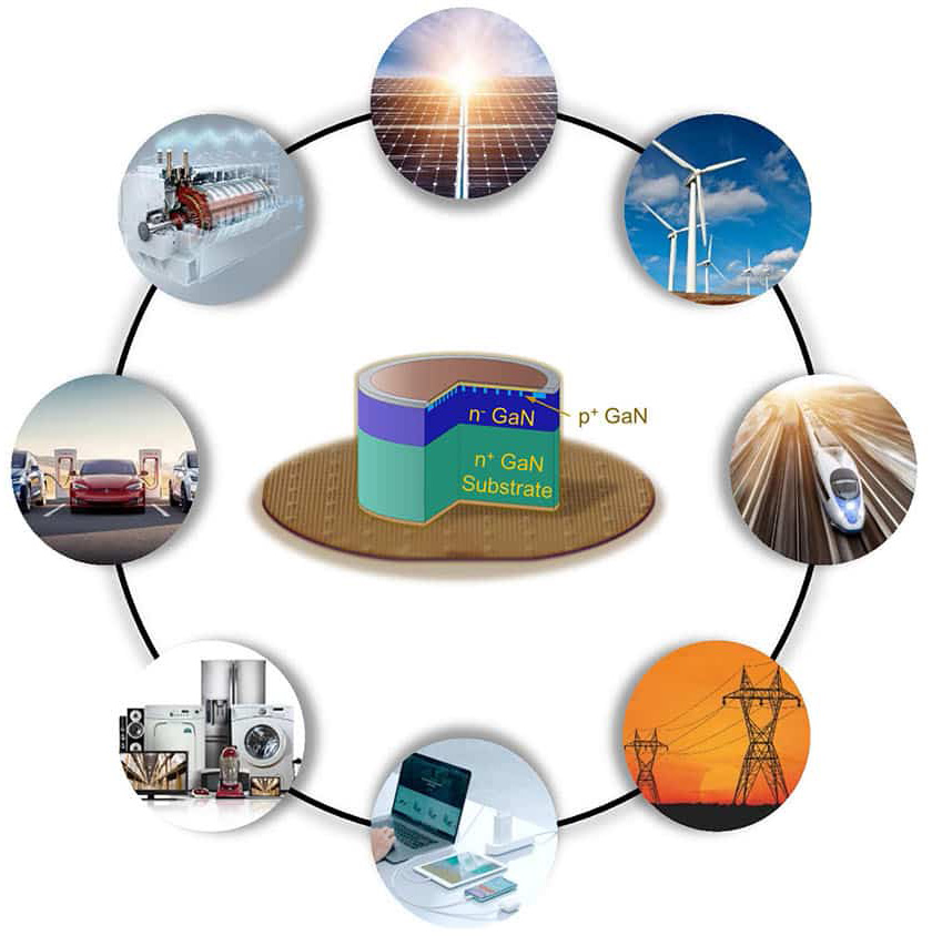
In a paper published in 2021, the researchers outlined a technique that uses ion implantation and activation to dope targeted areas in GaN materials. In the new paper, the researchers have demonstrated how this technique can be used to create actual devices. Specifically, the researchers used selectively doped GaN materials to create junction barrier Schottky (JBS) diodes.
“Power rectifiers, such as JBS diodes, are used as switches in every power system,” Collazo says. “But historically they have been made of the semiconductors silicon or silicon carbide, because the electrical properties of undoped GaN are not compatible with the architecture of JBS diodes,” he adds.
“We’ve demonstrated that you can selectively dope GaN to create functional JBS diodes, and that these diodes are not only functional but enable more power-efficient conversion than JBS diodes that use conventional semiconductors. For example, in technical terms, our GaN JBS diode, fabricated on a native GaN substrate, has record high breakdown voltage (915V [corresponding to a maximum electric field of 3.3MV/cm]) and record low on-resistance.”
The JBS has an ideality factor of 1.03, a turn-on voltage of 0.75V, and a specific differential ON-resistance of 0.6mΩ·cm2.
“We’re currently working with industry partners to scale up production of selectively doped GaN, and are looking for additional partnerships to work on issues related to more widespread manufacturing and adoption of power devices that make use of this material,” Collazo says.
The paper was co-authored by Spyridon Pavlidis, an assistant professor of electrical and computer engineering at NC State; Shashwat Rathkanthiwar, a postdoctoral researcher at NC State; Shane Stein, a Ph.D. student at NC State; Hayden Breckenridge, a former Ph.D. student at NC State; Erhard Kohn, a research associate at NC State and emeritus professor of Ulm University in Germany; Zlatko Sitar, Kobe Steel Distinguished Professor of Materials Science and Engineering at NC State and the founder of Adroit Materials; Will Mecouch, Seiji Mita, Baxter Moody, Pramod Reddy, James Tweedie and Ronny Kirste of Adroit Materials; and Kacper Sierakowski, Grzegorz Kamler and Michał Boćkowski of the Institute of High-Pressure Physics at the Polish Academy of Sciences.
The work was supported primarily by the US Department of Energy's Advanced Research Projects Agency-Energy (ARPA-E) as part of its PNDIODES program, under grants DE-AR0000873, DE-AR000149. The work received additional support from the US National Science Foundation, under grants ECCS-1916800, ECCS-1508854, ECCS-1610992, DMR-1508191 and ECCS-1653383; the Office of Naval Research Global’s Naval International Cooperative Opportunities in Science and Technology program, under grant N62909-17-1-2004; and Poland’s National Center for Research and Development (NCBR) under grant TECHMATSTRATEG-III/0003/2019-00.


