


News: Suppliers
8 September 2022
Clas-SiC qualifies Oxford Instruments’ contactless SiC plasma epi-prep
Oxford Instruments Plasma Technology (OIPT) of Yatton, near Bristol, UK recently announced the launch of its silicon carbide (SiC) substrate contactless plasma polishing solution to supersede the established chemical mechanical planarization (CMP) process with a clean, dry, lower-cost, higher-yield and sustainable alternative. The project has now taken a step forward through collaborating with Clas-SiC Wafer Fab Ltd of Lochgelly, Fife, Scotland, UK and qualifying whole-wafer 1200V MOSFET devices, further boosting confidence in the new solution and its impact on SiC power semiconductor devices.
“The 1200V MOSFET parametric results and yield are very encouraging, being very comparable to those of conventionally CMP-prepared wafers which were used as a direct comparison,” comments Clas-SiC’s technology & customer relations manager David Clark. “We rely on multiple vendors for substrates due to supply limitations, so incoming material variability is a challenge across the device manufacture industry. The fact that substrates were sourced, processed at Oxford Instruments, incorporated into our production flow on two separate device types and achieved such comparable results so soon should give Oxford Instruments confidence that their process window is robust and fit for purpose,” he adds. “For a first result this is a hugely positive outcome and gives confidence that Oxford Instrument’s new technology has a great future in reducing the cost of the very expensive incoming SiC substrates. This will be very important in reducing the cost of SiC-based power converters and in increasing their adoption in the marketplace.”
Demand currently exceeds supply for SiC substrates, and the wide-bandgap semiconductors that are manufactured on the substrates are also in short supply. This production gap is set to increase exponentially, as high-growth electric vehicle (EV) and sustainable energy markets incorporate ever increasing amounts of these compound semiconductors into their applications, so new solutions are needed. Oxford Instruments says that plasma polishing is a plug-and-play alternative to CMP that straightaway reduces the cost per wafer with reduced operating expenditure (OpEx), but is also a key enabling technology to accelerate the transition to thinner slices and more wafers per boule at wafer diameters of 150mm and 200mm. This, and other innovative SiC technologies, have the potential to shift the production paradigm, reckons OIPT, so that SiC supply chains can comfortably support high-growth technology markets in a sustainable way.
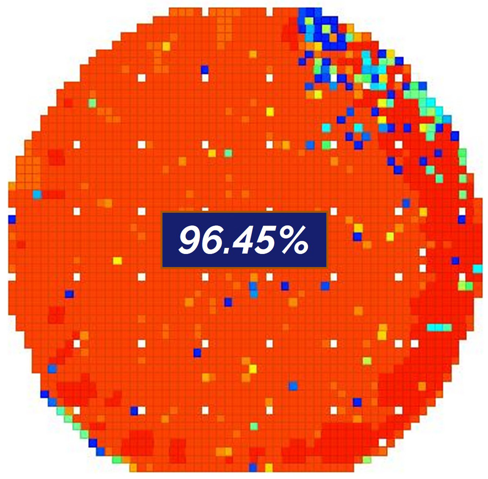
Picture: Clas-SiC’s micro-pipe density (MPD) device yield data.
Oxford Instruments is sharing full-wafer MOSFET performance data at the 19th International Conference on Silicon Carbide and Related Materials (ICSCRM 2022) in Davos, Switzerland (11-16 September), where there will also be an opportunity to speak in person at the event to discuss implementing plasma polish in high-volume manufacturing fabs. To prearrange an in-person meeting, contact Brian.Dlugosch@oxinst.com (VP of strategic production markets, Oxford Instruments Plasma Technology).
OIPT’s silicon carbide plasma epi-prep alternative to CMP validated
OIPT launches alternative to CMP for epi-prep of silicon carbide substrates


