News: Microelectronics
22 September 2022
Boron nitride pulsed laser deposition
Researchers in the USA report on pulsed laser deposition of hexagonal boron nitride (h-BN) on gallium nitride (GaN) with a view to optoelectronics and high-power electronics [Abhijit Biswas et al, Appl. Phys. Lett., v121, p092105, 2022]. The bandgap of h-BN is ~5.9eV, considered an ultra-wide bandgap (UWBG) relative to WBG GaN at ~3.4eV.
The team from Rice University, Oak Ridge National Laboratory and DEVCOM Army Research Laboratory found the h-BN/GaN to be second-harmonic generation active, and Schottky diodes formed from the material had a higher reverse-bias breakdown voltage, compared with Schottky diodes fabricated on GaN.
The researchers comment: “WBG and UWBG semiconductors including GaN, SiC, Al(Ga)N, diamond, Ga2O3 and BN are expected to revolutionize next-generation electronic device platforms because of their capabilities of realizing lower power loss, smaller system volume, higher operating voltage and temperature, and superior radiation hardness as compared to conventional semiconductors such as silicon and GaAs.”
The team also suggests: “As BN and GaN are both III-nitrides, the heterojunctions made of BN/GaN can modify and/or improve the GaN-based device performances and could play an important role in high-power electronics and radio frequency (RF) applications, up to subterahertz regimes.”
The PLD h-BN was grown on an unintentionally doped (UID) (0001) GaN on sapphire substrate produced through metal-organic chemical vapor deposition (MOCVD). The PLD growth temperature was 800°C. The laser source was a krypton fluoride (KrF) excimer laser emitting light of 248nm wavelength in the deep ultraviolet in 25ns pulses at 5kHz. The atmosphere was 100mTorr nitrogen. The laser ablation target was high-purity h-BN about 50mm away from the substrate.
The researchers see the advantages of PLD as including accurate stoichiometry transfer and uniform growth of films from dense poly- or single-crystalline targets with “enhanced adsorbate surface mobility endowed by high-energy radicals (both ionized and neutral; B+, N+, N*, N2, N2+ and BN) that are accelerated from the target in the form of laser-ablated plasma.” Also the growth temperature is relatively low, compared with MOCVD.
The 7nm BN layer resulted from 500 laser shots. After deposition, the sample was cooled at a rate of 20°C/min.
The BN layer was analysed using x-ray photoelectron spectroscopy (XPS). The analysis showed a main signal of B-N bonding, but there were also traces of bonds of B with oxygen and other B atoms. The N spectrum also showed the presence of some bonds with carbon impurities. Fourier-transform infrared (FTIR) and Raman spectroscopy studies, along with high-angle annular dark-field scanning transmission electron microscopy (HAADF-STEM) were also performed. Atomic force microscopy showed a surface roughness of 0.267nm, compared with 0.183nm for the substrate.
The atomic structure was found to be disordered in the Raman and HAADF-STEM analyses. The disorder was due to mismatching between the “a” lattice parameters: 2.50Å for BN and 3.18Å for GaN. The a-ratio of 3:4 is considered to be best for a hexagonal on wurtzite structure such as GaN. Since 3/4 of 3.18Å is 2.385Å, the BN lattice would need to be highly compressed with around 4.6% strain to obtain this ratio.
Instead, the researchers describe their BN layer as being “disordered, amorphous-like”. Even so, such material “was recently found to be applicable for ultraviolet (UV) photo-detection and high-performance electronics.”
Another potential opportunity could come from its optical second-harmonic generation (SHG). Since BN is transparent in the visible wavelength range, this could open the way to visible-range nonlinear optoelectronics. The SHG signal from the BN layer was found to be 2.2x that of the GaN substrate. The laser input was 800nm wavelength and the SHG response was at 400nm from the scanned surface. The SHG response was found to be uniform across the surface.

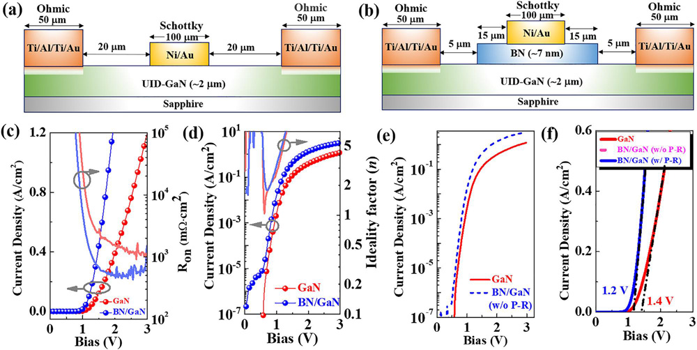
Figure 1: Schematics of (a) GaN and (b) BN/GaN Schottky diodes. Comparison of current density versus forward bias in (c) linear scale and (d) semi-log scale. (e) Comparison after removing the parallel resistance in BN/GaN diode. (f) Turn-on voltages from linear extrapolation.
The electrical performance was studied through fabricating nickel/gold Schottky diodes with and without the BN layer (Figure 1). The Ohmic metal contacts were titanium/aluminium/titanium/gold. The fabrication was performed at Rice University’s Nanofab Cleanroom facility.
The team comments: “It can be seen that the forward current of the BN/GaN device is higher than the GaN device, which suggests that the BN layer does not block the current compared with what an insulating layer does in a conventional metal-insulator-semiconductor diode.”
The BN/GaN device shows some leakage in the low-bias region, compared with the pure GaN diode. This can be modelled as a parallel resistance. Even removing this extra current, the BN/GaN device continues to show a higher current density for a given bias than the GaN diode.
The researchers extracted Schottky barrier heights of 1.3 and 1.1eV for the GaN and BN/GaN diodes, respectively. The respective idealities were 1.04 and 1.41.
The team writes: “The relatively lowered Schottky height of the BN/GaN diode not only leads to the increased forward current as compared with the GaN diode but also causes the increased reverse leakage current.”

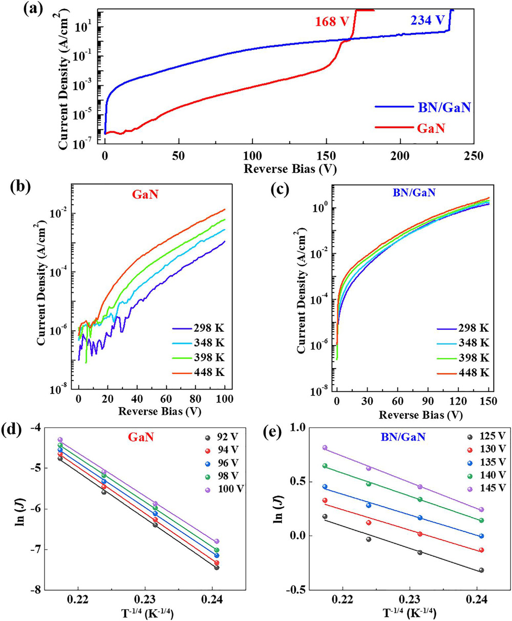
Figure 2: (a) Breakdown curves at room temperature. Reverse current density versus bias at different temperatures for (b) GaN and (c) BN/GaN Schottky diodes. VRH model plots for (d) GaN and (e) BN/GaN reverse leakage before breakdown.
Despite the high reverse-bias leakage, the BN/GaN diode had a higher breakdown voltage of 234V, compared with 168V for the GaN diode (Figure 2). The temperature variation of the performance was found to be consistent with the 3D variable range hopping (VRH) model, which predicts the current density at a given bias varying as J∝exp(-(Tc/T)1/4). Such behavior would be seen as a straight line on plot of the logarithm of current density (ln(J)) versus the inverse fourth root of temperature (T-1/4). The characteristic parameters Tc were extracted from the slopes of the straight lines: 1.5x10⁸K for GaN and 3.4x10⁵K for BN/GaN.
The researchers suggest the higher breakdown of the BN/GaN devices could be due to the higher critical field in BN, allowing high electric fields at the electrode edge where breakdown often occurs. Higher critical fields are expected in materials with wider bandgaps, although low purity and/or crystallinity can hamper this effect.
The author Mike Cooke is a freelance technology journalist who has worked in the semiconductor and advanced technology sectors since 1997.


