News: Optoelectronics
8 September 2022
Optically pumped yellow InGaN edge-emitting laser
University of California Santa Barbara (UCSB) in the USA claims the first report of optically pumped 568nm yellow lasing from a high-crystal-quality indium gallium nitride (InGaN) quantum well (QW) edge-emitting structure grown on bulk GaN substrate [Panpan Li et al, Appl. Phys. Lett., v121, p071103, 2022].
The researchers comment: “Even though, in practice, electrically injected laser diodes have broader applications and impacts, an optically pumped device is undoubtedly a good indicator that the material quality is competent for future development and can be well regarded as a precursor to electrically injected laser diodes.”
Yellow lasing is quite difficult in general, depending on frequency conversion in gas, ion or dye media. Such methods tend to be bulky, expensive and inefficient. Use for yellow laser light has been found in advanced biology and astrophysics/astronomy studies.
The problems for generating yellow light from InGaN include the large lattice mismatch between GaN and high-indium-content InGaN and inconvenient electric fields arising from differing charge polarization of the various III-nitride bonds. In laser structures, there is the additional problem of arranging suitable confinement of the optical mode to enable stimulated emission. The UCSB team points to the aluminium gallium nitride (AlGaN) cladding that is often used being problematic in the yellow range due to the thickness required going beyond the critical thickness, after which the material relaxes by cracking.
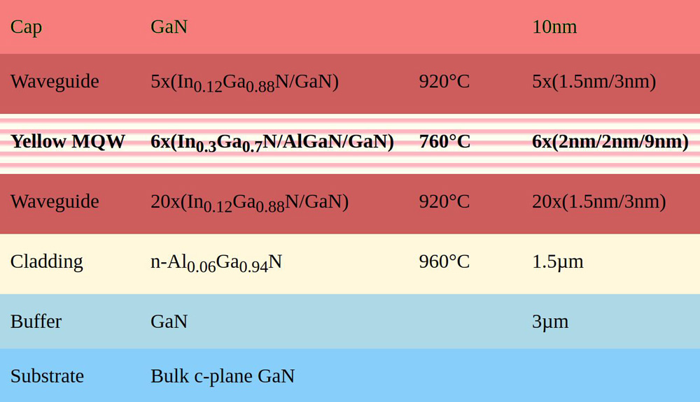
The laser material was grown by atmospheric-pressure metal-organic chemical vapor deposition on c-plane bulk GaN (Figure 1). The yellow light was generated by high-indium-content InGaN multiple QWs (MQWs) separated by AlGaN/GaN barriers.

Figure 1: Epitaxial structure.
The researchers were keen to have a very flat surface to increase the optical pumping efficiency. Atomic force microscopy gave a 0.3nm root-mean-square roughness over a 5μmx5μm field. The threading dislocation density was estimated to be 5x10⁷/cm2 through analysis of cathodoluminescence images. The substrate threading dislocation density was of order ~106/cm2. The team points to the low-temperature growth of the lattice-mismatched MQW as the main source of the extra threading dislocations.
The normal top cladding was replaced by a quarter-wavelength layer of titanium dioxide (TiO2). “Compared with traditional epitaxial InGaN waveguiding and AlGaN cladding, the use of the high refractive index of TiO2 (near 2.6 at 580nm) on the top of the active regions greatly improves the confinement in the vertical direction by attracting the mode upward, although such structure will not be valid for electrical injection of laser diodes,” the team explains.
The TiO2 does have the drawback of absorbing the pump wavelength of 355nm, but the coefficient is less than that of high-indium-content InGaN. The 51nm quarter-wavelength TiO2 cladding was deposited on a 38nm tantalum oxide (Ta2O5) top waveguide layer. On the basis of simulations, the team suggests that “the combined use of Ta2O5 and TiO2 layers can enhance the confinement factor by nearly 25% while keeping the internal loss and single-pass absorption of the pumping source still at the same level.” These top layers were applied by ion-beam deposition.
The laser bars were formed by reactive ion etch of 20-50μm ridges. The material thickness was reduced to 75μm by polishing. The bars were cleaved to give mirror facets, and then mounted on copper heatsinks.

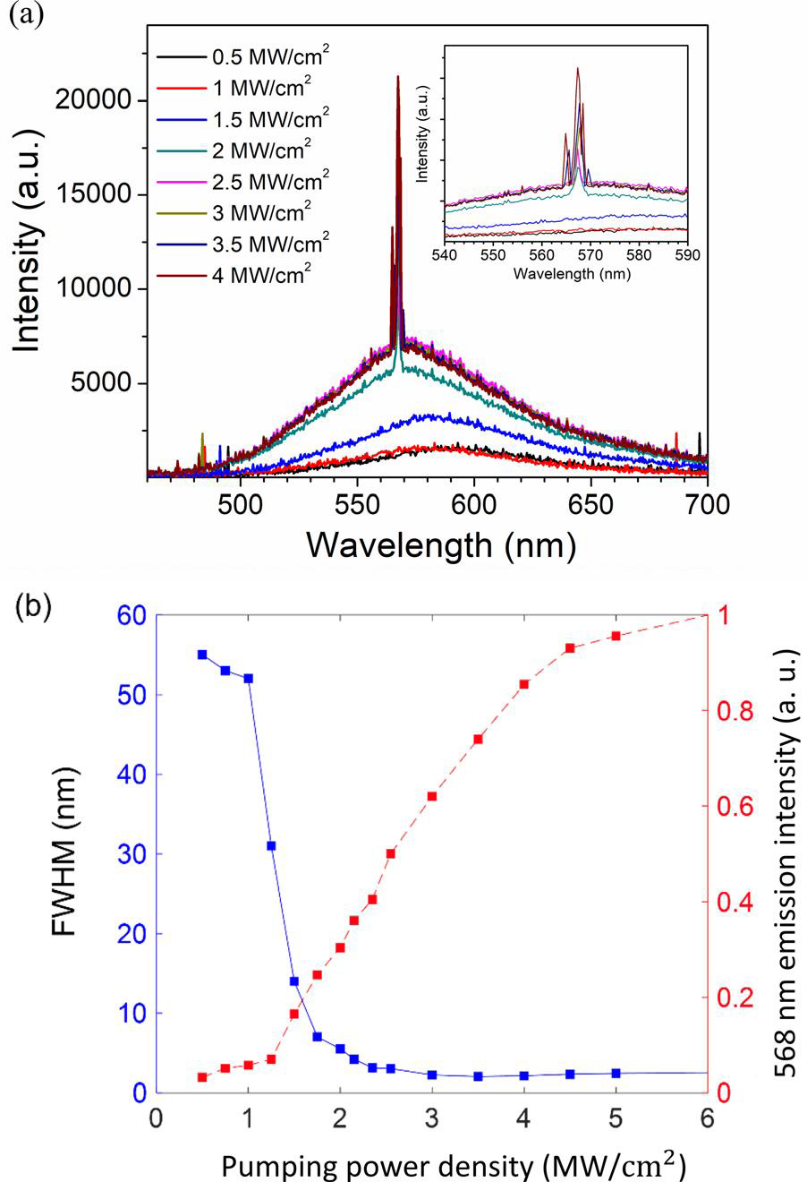
Figure 2: (a) Spectra collected at laser facet at various pumping power densities. Inset: close-up of stimulated emission wavelength. (b) Full-width at half maximum (FWHM) and intensity of simulated emission versus pumping power density.
The peak emission for a 1.4mmx50μm laser bar was at 568nm under 10Hz 30ps pulsed pumping (Figure 2). As the pumping passed through the 1.5MW/cm2 pump power threshold the line-width reduced from 50nm to less than 2nm. The polarization of the laser light was found to be more than 90% transverse electric, as expected from simulations.
The author Mike Cooke is a freelance technology journalist who has worked in the semiconductor and advanced technology sectors since 1997.


