


News: Microelectronics
6 April 2023
Progress towards complementary GaN on silicon
Researchers in the USA, Bangladesh and the United Arab Emirates report progress in developing complementary transistor technology (CT) on a metal-organic chemical vapor deposition (MOCVD) gallium nitride (GaN) on silicon (Si) substrate platform [Qingyun Xie et al, IEEE Transactions on Electron Devices, v70, p2121, 2023].
The team from Massachusetts Institute of Technology in the USA, Bangladesh University of Engineering and Technology, and Technology Innovation Institute in the United Arab Emirates, report: “To the best of the authors’ knowledge, the best p-FET in this work features the highest current density among MOCVD III–N p-FET (>2× the previous record, −140mA/mm), as well as competitive performance compared with GaN/AlN molecular beam epitaxy (MBE) counterparts”
The p-channel field effect transistors (p-FETs) were integrated with n-FETs with a view to wafer-level heterogeneous integration of GaN complementary circuits (based on a silicon substrate) with silicon complementary metal–oxide semiconductor (CMOS) technology to achieve multi-functional chips.
Complementary circuits using p-FETs and n-FETs in enhancement mode (normally off) reduces static power consumption, and has been key to the success of mainstream silicon electronics. Transferring this capability to GaN could extend their reach beyond compact, efficient power management — deployed in data centers, power adapters, electric vehicles (EVs), and 5G/6G telecommunications — to more sophisticated applications requiring control loops and analog mixed-signal blocks. The use of p-FETs in GaN circuits could also enable higher switching speeds for more efficient and higher-density power converters.
The researchers found that scaling the p-FETs with reduced gate length (LG) greatly improved the maximum drain current (ID,max) performance: “The p-FET of this work achieved −ID,maxxLG = 52.5μA, which is a record for MOCVD-based (single GaN/AlGaN epitaxial layer) p-FETs, and is close to the values for the record MBE-based p-FETs and MOCVD superlattice (multiple GaN/AlGaN epitaxial layers) p-FETs.”
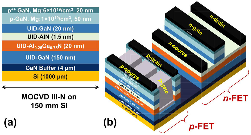
Figure 1: (a) Epitaxial structure. (b) Device structures of p-FET (SA FinFET) and n-FET (SA-gate p-GaN-gate HEMT)
The wafers for the transistors were supplied by Dr Kai Cheng of China-based Enkris Semiconductor Inc. The epitaxial structure was grown on 6-inch silicon wafers (Figure 1). A 1.5nm AlN layer was inserted to boost hole mobility through charge polarization effects from the ionic nature of the III–V chemical bond. The AlN also served as an etch-stop layer in the device fabrication processes.
The p-FET devices used a fin architecture to enable channel scaling in an effort to overcome the low, less than 30cm2/V-s hole mobility in GaN. The fin structure also improved acceptor ionization, increasing hole density, through the polarization-induced fields.
The fabricated was carried out at MIT’s own facility with some work being carried out at Rensselaer Polytechnic Institute in the USA by Bryant C. Colwill. The p-FET fabrication used a self-aligned (SA) process with the ohmic nickel/gold/nickel metal source/drain electrodes being applied first to also serve as part of the masking and alignment for subsequent etching of the fin channels and gate structures.
The fin patterning was through electron-beam lithography on hydrogen silsesquioxane (HSQ) resist. The fins were etched through reactive-ion etch (RIE). The fin direction was chosen to be in the m-plane, ensuring smoother sidewalls. Further steps were taken to reduce etch damage, in particular, tetramethylammonium hydroxide (TMAH) exposure at 75°C for 5 minutes, and 500°C annealing in nitrogen atmosphere for 30 minutes. These treatments were found to reduce channel on-resistance (RON) by 15%.
The researchers report: “The optimized process was capable of achieving the fin widths of 20nm at an LSD of <200nm. The SA architecture ensures that the access region (and therefore access resistance) is negligible, and that the entire length of the fin (=LSD) is gated.”
The gate stack consisted of atomic layer deposition (ALD) of 15nm silicon dioxide (SiO2) and radio frequency (RF) sputtering of titanium/gold gate metals. The 250°C ALD oxide came from tris(dimethylamino)silane (TDMAS) and O2 plasma precursors.
The best p-FET device demonstrated a maximum drain current of −300mA/mm, 27mΩ-mm RON, 3V threshold, and 13mS/mm peak transconductance. The on/off current ratio was only 200 due to gate leakage through the dielectric. The poor oxide quality also impacted gate control and drain-induced barrier lowering (DIBL). Destructive breakdown occurred around 20V.
The p-FETs were affected by the gate recess depth, where a second threshold was seen with deep recessing. Simulations suggest that the second threshold comes from a second bulk sub-channel forming in addition to the desired two-dimensional hole gas (2DHG) channel near the p-GaN/AlGaN interface. In deeply recessed structures the overlying p-GaN is thinner, reducing hole concentrations and the transconductance of the 2DHG sub-channel.
The researchers comment: “The p-channel in the epitaxial structure is buried, and therefore a simple top gate is not sufficient to exert electrostatic control over the entire channel. A recessed gate structure, while adding design flexibility to p-FETs, requires special consideration in the design (recess depth and geometric profile) and fabrication (e.g. reducing etch-induced damage).”
For the n-FET a gate-first SA strategy was used. The p-GaN gate structure was masked using patterned nickel/gold/nickel on a blanket layer of sputtered tungsten. Tungsten has high thermal stability and forms a Schottky contact with p-GaN.
The p-GaN not under the gate structure was then selectively etched away before application of the titanium/aluminium/nickel/gold source/drain electrodes. The gate stack was placed in the middle of the source/drain gap, and there were no electric field management structures to improve performance. The resulting devices are therefore described by the team as ‘proof of concept’.
N-FET devices with 200nm gate length showed good saturation with 525mA/mm maximum drain current and 2.9mΩ-mm RON. The threshold was positive at +1.6V, giving enhancement-mode, normally-off performance. The peak transconductance (g2) of 265mS/mm “reflects good gate control using the proposed gate metallization stack”, the team comments. Destructive breakdown occurred at 50V.
The device structure had improved performance when fabricated on an epitaxial structure not designed to support p-FETs. In particular, the 1.5nm AlN and 20nm GaN layers were not present, and the AlGaN was reduced from 20nm to 15nm: the drain current reached 750mA/mm with 1.3mΩ-mm RON. The sub-threshold swing was also reduced from 123mV/decade (with AlN/GaN insertions) to 100mV/decade (without). The closer proximity of the gate to the channel improved the electrostatic control.
The researchers benchmarked their work against other reports working towards similar complementary technology goals (Figure 2). The team particularly highlights reports where the p- and n-FET were produced on the same platform. The researchers point out that all these reports used MOCVD rather than MBE. The MIT et al devices had a ratio of the maximum drain current of the n-/p-FET of 1.75, closer to unity than the other reports. The p/n-FET ratio for RON was 9.3, obviously quite far from 1, but only one other report was inside that.
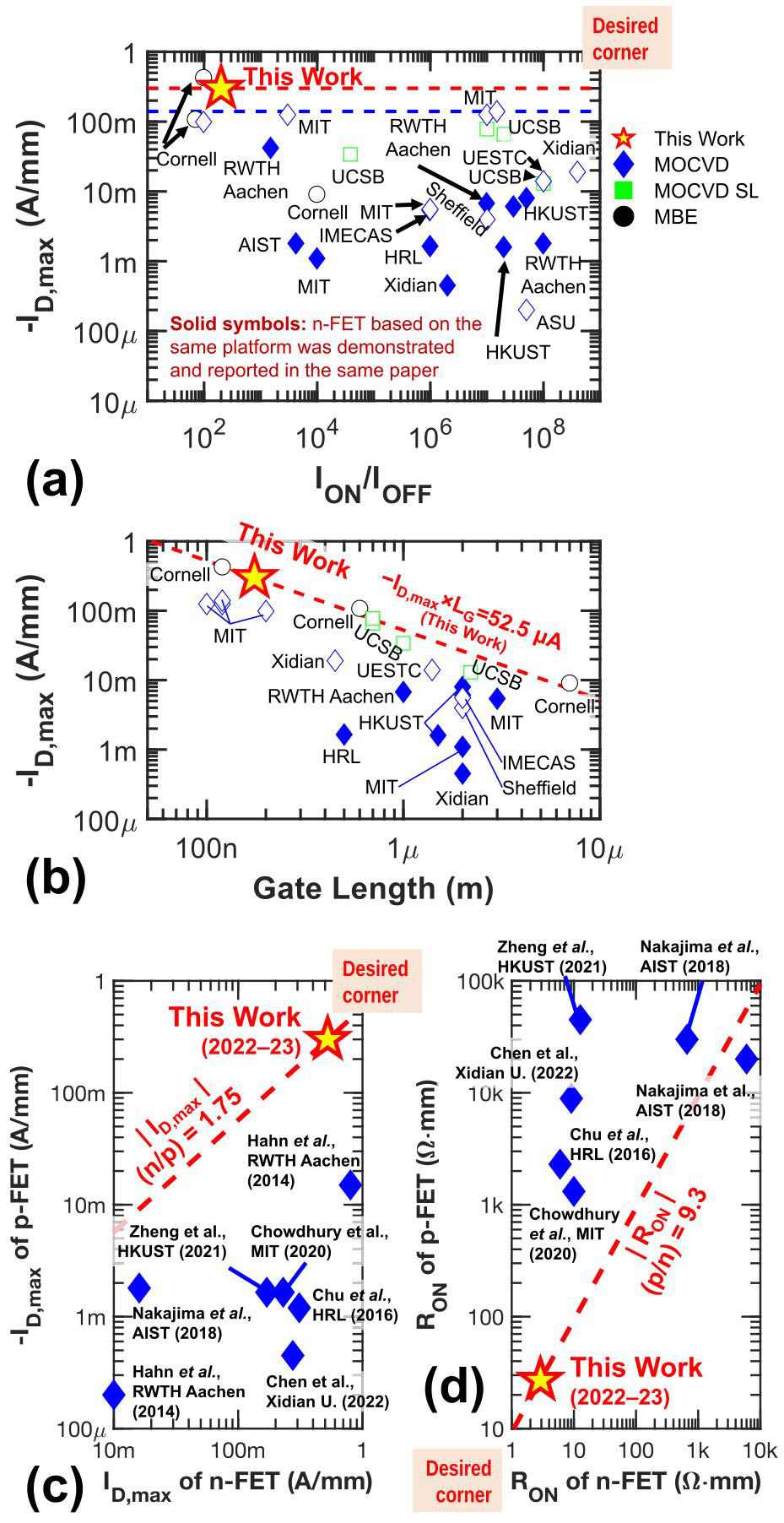
Figure 2: Benchmarks with other published works. (a) GaN p-FETs in terms of ON-current and ON/OFF ratio. (b) Trade-off between current density and gate length. (c) and (d) GaN CTs (complementary transistors reported in same article) in terms of current densities and RON, respectively. Solid symbols indicate complementary transistors (p-FET and n-FET) on the same platform demonstrated and reported in the same article.
The researchers comment: “A ratio approaching unity (=1) is desired to achieve reasonable transistor sizing. The current density of the reported GaN CT is comparable with that of 5V-rated silicon CMOS in an industry 0.13μm bipolar-CMOS−DMOS (BCD) process published in 2016 (ID,max{n, p} = {520, −323}mA/mm).”
The author Mike Cooke is a freelance technology journalist who has worked in the semiconductor and advanced technology sectors since 1997.


