


News: Suppliers
7 February 2023
ams OSRAM qualifies Aixtron’s G5+ C and G10-AsP systems on 200mm wafers for micro-LEDs
Deposition equipment maker Aixtron SE of Herzogenrath, near Aachen, Germany says that ams OSRAM GmbH of Premstaetten/Graz, Austria and Munich, Germany has qualified its AIX G5+ C and G10-AsP (arsenide–phosphide) metal-organic chemical vapor system (MOCVD) systems on 200mm wafers for a micro-LED application.
The AIX G5+ C and the new G10-AsP apply Aixtron’s planetary technology for high-resolution micro-LED displays. In spring 2022, ams OSRAM had announced plans to create additional manufacturing capacity in 200mm for the production of LED and micro-LED at its existing location in Malaysia. The MOCVD systems are expected to help enable volume production of micro-LEDs for a new generation of display applications.
“Aixtron and ams OSRAM have a long-standing cooperation, and we are familiar with the performance and quality standards of the equipment. For an ambitious project like the development and production of micro-LED for AsP and GaN devices, we needed exactly such a partner at our side,” says Robert Feurle, executive VP & head of ams OSRAM’s Opto Semiconductors business unit.
“The G10-AsP and AIX G5+ C qualification at ams OSRAM is a very important milestone in our company’s history,” says Aixtron’s CEO & president Dr Felix Grawert. “ams OSRAM is a world-class LED manufacturer and perfectly positioned to enable the fundamental new technology that will come to market,” he adds. “We are on the verge of a technology shift away from conventional display technologies to a new type of micro-LED displays. Now, Aixtron is entering one of the future’s growths markets that has an enormous potential, and we are doing this with a perfect partner at our side.”
Micro-LED technology is said to offer significant advantages for display technology such as higher pixel density, longer lifetime, higher brightness, faster switching speed and a wider color spectrum. A key benefit is also the low relative energy consumption, qualifying micro-LEDs for upcoming generations of smaller display-equipped consumer devices that provide a very limited space for batteries.
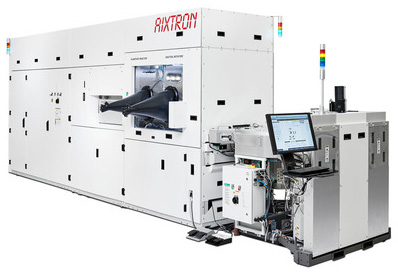 Picture: Aixtron’s new G10-AsP MOCVD system, said to be the first fully automated AsP reactor offering cassette-to-cassette wafer loading as well as a cleaning mechanism based on in-situ etching.
Micro-LED volume production involves a special transfer process where many thousands of LED chips (arrays) of just microns in size are picked up and transferred. Any defect can result in dead pixels, which can make an entire array useless. Hence, an almost error-free epitaxy process is necessary, minimizing defects and allowing for high yield and economically viable production of micro-LEDs.
Aixtron says that its new G10-AsP epitaxy tool has been designed to address the specific needs of this application. It is claimed to be the first fully automated AsP reactor offering cassette-to-cassette (C2C) wafer loading as well as a cleaning mechanism based on in-situ etching. Together, these two features are said to have a major impact on yield performance. The system also offers the advantages of batch reactor technology: it comes with what is claimed to be the lowest production cost per wafer currently available in the market and the highest throughput per cleanroom area. At the same time, the new tool comes with precise flow and temperature control, optimizing material uniformities run after run.


