


News: LEDs
16 February 2023
InGaN micro-LEDs for full-color passive-matrix displays
Matthew Hartensveld of Innovation Semiconductor Inc reports on a demonstration of indium gallium nitride (InGaN) micro-light emitting diodes (μLEDs) integrated in a full-color 5x5 passive matrix [IEEE Electron Device Letters, published online 16 January 2023].
The color tunability was arranged through deliberate incorporation of spontaneously-formed V-grooves in the μLED wafers, as previously reported here [Mike Cooke, Semiconductor Today, 12 August 2022], based on Hartensveld’s work last year.
The V-grooves cut through the light-emitting InGaN/GaN multiple quantum wells (MQWs) locally altering the band structure. When incorporated into μLEDs the color of the emitted light changes according to the injected current density.
Such optoelectronic behavior is of much interest for full-color display deployment in high-resolution augmented reality (AR) and other systems. Using one device type covering the full color range, rather than integrating a series of separate devices, usually in incompatible III-V technologies, to cover red-green-blue (RGB) emissions, should reduce complexity and hopefully lead to lower production costs and so on.
The μLED wafers included buffer layers strained to optimize V-groove formation in the overlying InGaN/GaN MQW structure.
The wafer growth was on sapphire, using metal-organic chemical vapor deposition (MOCVD). The structure was designed to target green wavelength emission in the planar region away from the V-grooves.
As usual, there were n-GaN contact and p-GaN layers below and above the MQWs, respectively. Electrons were blocked from overshooting the MQW by a p-type aluminium gallium nitride (p-AlGaN) electron-blocking layer (EBL) between the MQW and p-GaN.
Scanning electron microscopy (SEM) and transmission electron microscopy (TEM) found a random V-groove density of 4x10⁸/cm2.
The passive array fabrication began with mesa isolation into cathode-connected 25μ-wide columns by etching down to the sapphire substrate, forming the base of the 5x5 array of 20μm2 μLEDs (Figure 1). The n-contacts and individual μLEDs were created by etching cuts through the anode isolation, provided by 300nm plasma-enhanced chemical vapor deposition (PECVD) silicon dioxide (SiO2). The anode contacts were realized by sputtering and etching 100nm indium tin oxide (ITO) transparent conductor and deposition of and lift-off of titanium/aluminium row lines and n-contact pads.
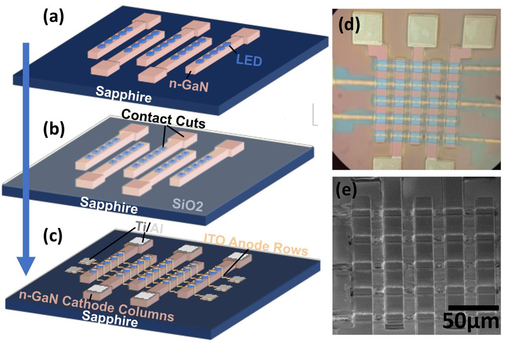
Figure 1: (a) Formation of n-GaN columns with μLEDs, (b) oxide deposition and contact cut formation for anode and cathode connections, (c) formation of ITO anodes and Ti/Al contact pads, (d) optical image of 5x5 array, (e) SEM image of 5x5 array.
The turn-on voltage at 8V was high compared with the ~1.5V for previous reports on V-groove μLEDs. Hartensveld blames “lack of optimized metallization for both the n-type and p-type contacts, where there is an added voltage drop particularly from the p-type contact.”
In particular, ITO is n-type conducting, giving a tunnel junction injection of holes into the μLED. “If the ITO deposition and annealing process is not optimized, the reversed p–n junction between the n-type ITO and p-GaN must be first overcome, leading to the voltage drop,” Hartensveld explains. In addition to improved annealing, a different choice of metal electrode, e.g. nickel/gold, could enhance efficiency.
The first emissions after turn-on were red but, at higher voltages and hence current injection, the color changed successively until reaching blue. The current density for 640nm red emission was ~1x10⁻⁵mA/cm2; and that for 425nm blue ~8x10⁻⁴mA/cm2.
Of course, the higher voltage/current leads to higher brightness. Normalizing to the red brightness level could be achieved through pulsing the drive current for the shorter wavelengths of green and blue, at a duty cycle around 1% and 0.1%, respectively. “Color uniformity in the critically important color red was demonstrated across the array,” Hartensveld reports.
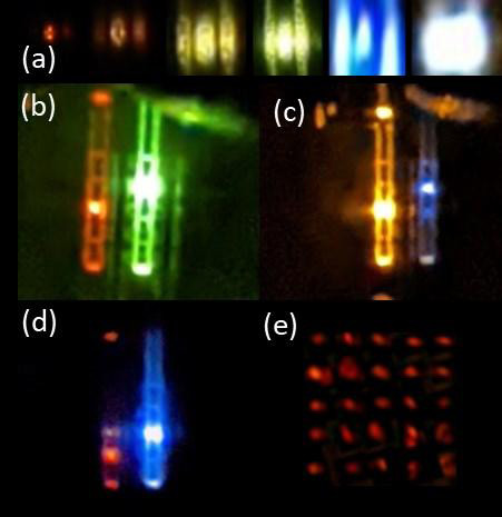
Figure 2: (a) Differing colors generated from a single μLED; the last image in the strip is ‘white’ generated by mixing blue and yellow emissions appropriately. (b) Red and green, (c) yellow and blue, and (d) red and blue emission from two μLEDs, (e) 5x5 μLEDs in red sequentially generated through individual driving and image captures.
The color gamut of the devices is somewhat let down in the green region. Hartensveld comments: “Due to the single μLED color tunable pixels compared with the conventional three fixed μLED approach, a parabola-shaped coverage of the color space is created. Both blue and red have good positioning near the edges of the chart, with further optimizations possible for green.”
The author Mike Cooke is a freelance technology journalist who has worked in the semiconductor and advanced technology sectors since 1997.


