


News: Optoelectronics
23 February 2023
Indium arsenide quantum dot lasers on silicon with simple GaAs buffer
Researchers in China have fabricated monolithic indium arsenide (InAs) quantum dot(QD) lasers on silicon (Si) without using dislocation filter layers of strained-layer superlattices (SLSs) in the gallium arsenide (GaAs) buffer [Yongli Wang et al, Optics Express,v31, p4862, 2023].
The team from Institute of Semiconductors, University of Chinese Academy of Sciences, and Beijing University of Posts and Telecommunications, comments: “This simple structure avoids the injection of current through the SLSs interface and the cross-hatching introduced by the SLSs. Moreover, the whole process can be further simplified, which is expected to promote the application of photonic integrated circuits.”
The purpose of dislocation filters, and other complex techniques is to avoid defects that sap laser performance such as antiphase boundaries (APBs) and threading dislocations, which arise through the differences in the charge polarities of the chemicals bonds, and the large lattice mismatch, between silicon and GaAs.
The researchers add: “As the device has GaAs-only growth and has a buffer as thin as ~2.5μm, the compatibility of the device with the industry-standard fabrication process has also improved.”
The team sees their approach as providing “an innovative way to prepare low-cost, CMOS-compatible silicon-based light sources, which is conducive to promoting the commercial development of silicon photonic interconnects.”
The GaAs buffer was grown using metal-organic chemical vapor deposition (MOCVD). The silicon substrate was cleaned using an RCA process modified with a sulfuric acid (H2SO4) step to remove organic pollutants, particles, metal contaminants, and native oxide. A 735°C, 20min surface treatment with hydrogen (H2) and arsine (AsH3) promoted atomic reconfiguration into double-atom steps to enable GaAs growth avoiding APB formation.
The unintentionally doped (uid) GaAs buffer itself was grown in three temperature steps — 420°C, 630°C and 700°C. The low-temperature step was critical in suppressing APBs and reducing threading dislocation density (TDD), according to the team. The researchers also used thermal cycle annealing (TCA) to encourage dislocation annihilation. The TCA consisted of two periods of three cycles of 720°C/450°C alternations.
Atomic force microscopy (AFM) gave a surface roughness of the buffer of 2.85nm. The TDD was estimated at 9.2x10⁶/cm2 from x-ray diffraction analysis. A very similar result was found from electron channeling contrast imaging (9.4x10⁶/cm2). Using more complex techniques, TDDs of 1.5x10⁶/cm2 have been achieved.
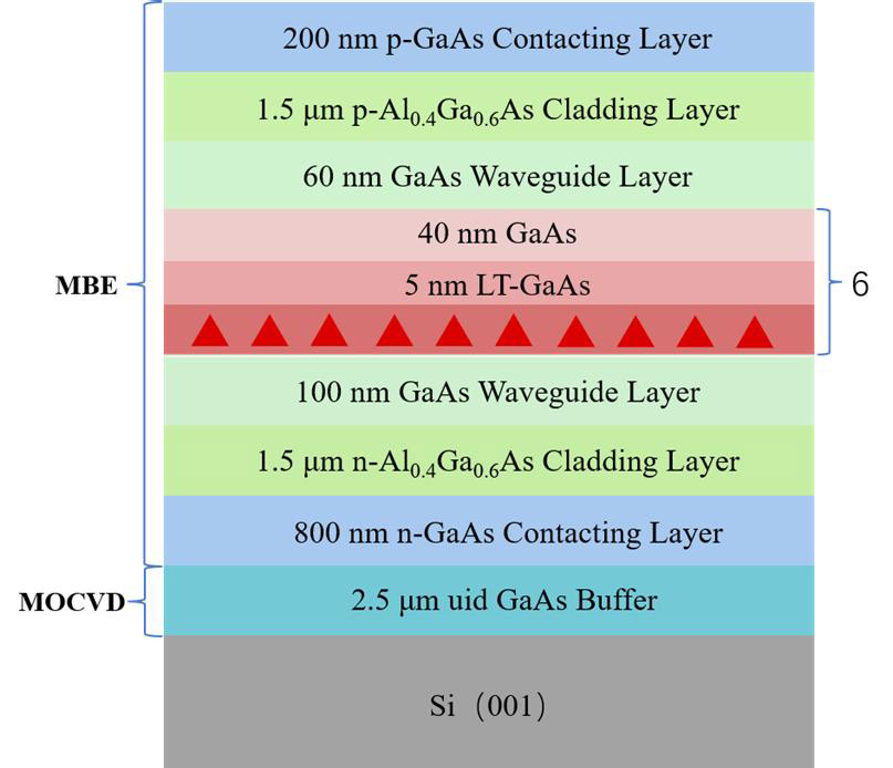
Figure 1: Schematic of InAs/GaAs QD laser material grown on on-axis Si (001).
Further growth (Figure 1) was by molecular beam epitaxy (MBE). The active light-generating region consisted of six layers of InAs quantum dots (QDs) in GaAs. The QD density in each layer was around 5.2x10¹⁰/cm2, according to AFM. A photoluminescence peak for the InAs QDs was observed at 1296nm wavelength with 34meV full-width at half maximum (FWHM). Optical confinement was provided by aluminium gallium arsenide (AlGaAs) cladding layers.
The material was fabricated into broad-area laser diodes (LDs) with silicon dioxide (SiO2) electrical isolation. The p- and n-electrode metal sequences were titanium/platinum/gold and gold-germanium alloy/nickel/gold, respectively. The devices were thinned to about 100μm. There was no coating applied to the cleaved facets.
A laser diode with 2mmx50μm ridge had a room-temperature laser threshold current at 397mA (397A/cm2 density) in continuous wave (CW) operation. The single-facet output power reached 138mW at 2A, while the slope efficiency was 0.085W/A. The power-current performance showed kinks due to mode competition.
University of California Santa Barbara (UCSB) has achieved 185mW and 175mW output power for InAs QD laser diodes with and without facet coatings, respectively, on a complex buffer.
Spontaneous emission at 300mA, below threshold, had a wavelength of 1302nm with 27nm FWHM. At increased 600mA injection, above threshold, the FWHM narrowed to 2.7nm, while the emission wavelength redshifted somewhat.
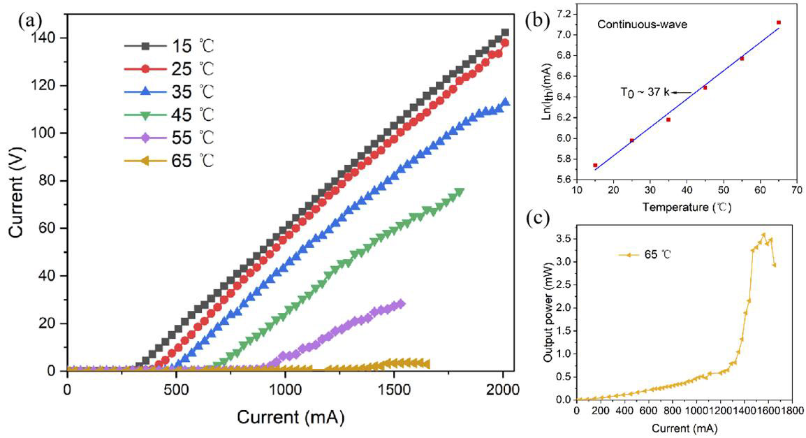
Figure 2: (a) High-temperature measurements of device showing lasing up to 65°C under CW operation. (b) Natural logarithm of threshold current versus temperature. (c) Output power versus injection current at 65°C.
The device continued to lase, demonstrating a maximum 3.6mW output power, when the heatsink temperature was raised to 65°C (Figure 2). The degradation of the laser threshold with increased temperature had a characteristic temperature (T0) of 37K between 15°C and 65°C. The researchers suggest that T0 could be increased with a p-type modulation doping, but this would have to be balanced against that technique’s tendency to increase threshold current.
The author Mike Cooke is a freelance technology journalist who has worked in the semiconductor and advanced technology sectors since 1997.


