


News: Microelectronics
2 February 2023
Surge handling of GaN polarization superjunctions
University of Sheffield in the UK and Japan-based Powdec K.K. have presented surge current capabilities of 1.2kV gallium nitride (GaN) polarization superjunction (PSJ) diodes “for the first time” [Alireza Sheikhan et al, Jpn. J. Appl. Phys., v62, p014501, 2023].
The team comments: “The results show that GaN PSJ diodes can be highly cost-effective and reliable for high-frequency, high-efficiency power electronic designs.”
The researchers add: “One of the key parameters of power diodes is their surge current capability, which is a requirement in cases such as fault occurrences within a system or inrush current during starting phase.”
It is hoped that GaN-based circuits will enable faster power switching, allowing the use of smaller magnetic components, such as inductors and transformers, at higher power density. The implementation of superjunction conductivity modulation schemes, as commercially implemented in silicon, allows devices to beat the theoretical material limits of simple one-dimensional device models.
The researchers used an aluminium gallium nitride (AlGaN) layer sandwiched between two GaN layers to create two-dimensional hole (2DHG) and two-dimensional electron (2DEG) gases at the respective GaN/AlGaN interfaces due to piezoelectric and spontaneous charge polarization fields due to the ionic nature of the III-N chemical bonds (Figure 1). “The device uses the concept of polarization charge balance to achieve a flat distribution of electric field resulting in an enhanced blocking voltage capability,” the team explains.
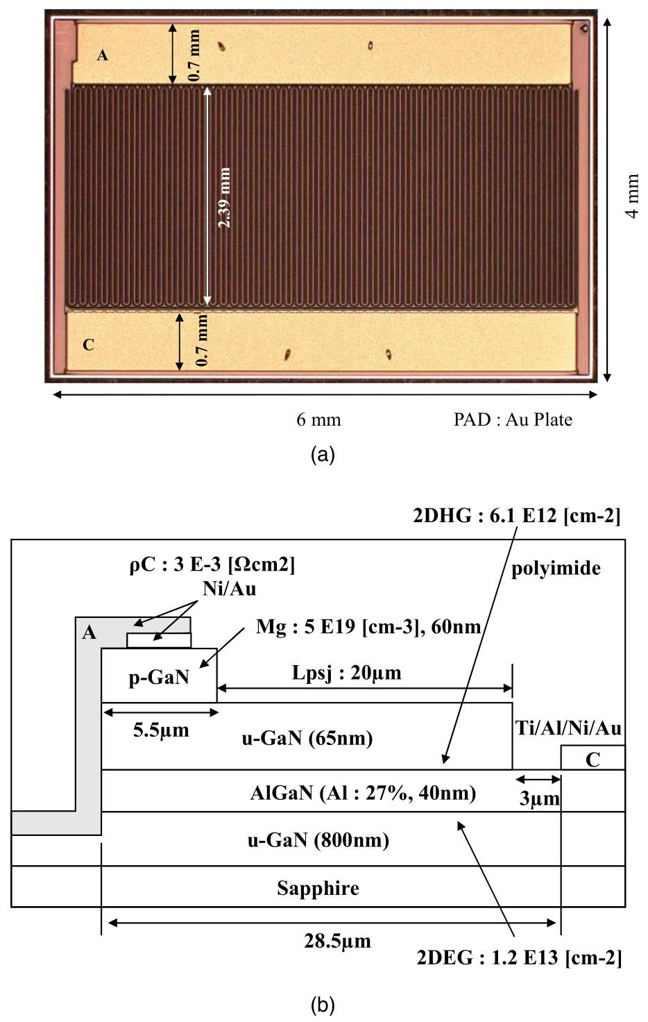
Figure 1: (a) Top view of 1.2kV GaN PSJ diode chip and (b) cross-sectional schematic structure.
The anode (A) and cathode (C) contacts were interdigitated with 47 and 48 fingers, respectively, resulting in a 2.39mm diode width. The anode contact was doped with magnesium (Mg) to give p-type conductivity. The anode electrode was nickel/gold (Ni/Au), and the cathode had added titanium (Ti) and aluminium.
The drift region was 20μm long (Lpsj). This parameter controls the voltage-blocking capability of 1.2kV and gives a breakdown around 2kV.
Reverse bias removes the polarization charges from the drift region, with the holes leaving through the anode and the electrons leaving through the cathode. The researchers comment: “The absence of polarization charges results in an even distribution of electric field, enabling extremely high reverse voltage blocking capability superior to conventional GaN HEMTs.”
The depletion of the drift region was seen in 1MHz capacitance measurements, which showed a decrease from 12nF at 1V reverse bias in two steps before 5.5V, which the team attributed to the 2DEG being removed first and the 2DHG second. The capacitance at 1200V was 34pF.
In forward bias, current flows through the 2DEG once the Schottky barrier of around 1V is exceeded. “Due to the high bipolar on-set voltage of 3.4V of the anode junction at room temperature and the very low resistance offered by the 2DEG beneath the 2DHG region, the PiN diode does not turn on under normal conditions,” the team adds.
Under 250μs pulsed operation of 160ms period, the forward current saturated at 76A at 25°C. The slope resistance was 125mΩ and the turn-on came at 0.9V. At 1.6V the current was 5A. The 5A forward voltage increased to 2.2V at 175°C. At the higher temperature the slope resistance also increased to 239mΩ.
The researchers comment: “Despite having a merged PiN and Schottky configuration, the GaN PSJ diode behaves like a pure Schottky diode without a bipolar mode of operation. This is entirely due to the low resistance of the 2DEG beneath the 2DHG region, ultra-short lifetime of holes and high bipolar on-set voltage.”
The reverse recovery charge (Qrr) in switching from forward to reverse bias was 45nC at 6A load. The softness factor was 0.6, the ratio of the restoration time to the overshoot time. Factors less than one are often described as “snappy”. The peak reverse current was -4.35A. The total reverse recovery time was 20ns.
The surge handling capability was measured using 10ms half-sine forward current pulses (Figure 2). The device survived at currents up to 60A, nearly 8x the rating of the device, according to the researchers. The maximum deposited surge energy was calculated at 5.4J.
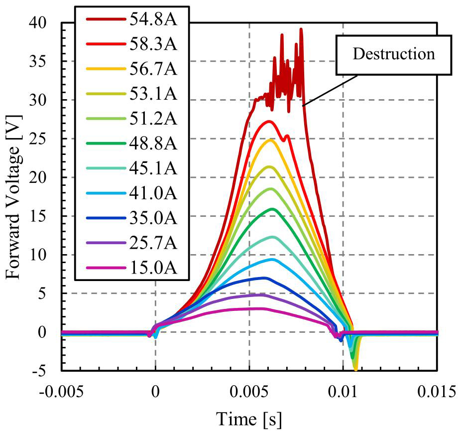
Figure 2: Voltage wave forms (VAC) of GaN PSJ diode at different surge current conditions.
At 58.3A, a secondary peak appeared when the forward voltage dropped to around 25V, which the team attributes to activation of the bipolar operation mode. Thermal effects were seen with the forward voltage being higher for a given current in the return to zero part of the pulse.
The team explains: “The inrush of minority carriers (holes) from the p-GaN region due to activation of the bipolar mode leads to device degradation. The bipolar operation is only observed in the return/falling branch, which is due to the temperature dependency of the bipolar on-set voltage, which reduces due to self-heating.”
After the 58.3A stress, the device was only capable of handling 54.8A before destruction. The team comments: “The rising branch shows a significant degradation in current due to the partial damage from the previous surge current pulse of 58.3A.”
After 51A surge stress, the device showed a slight drop of forward current for given forward voltage, of order 2A at 20V. Meanwhile, the reverse current leakage increased by about 10% at 1200V.
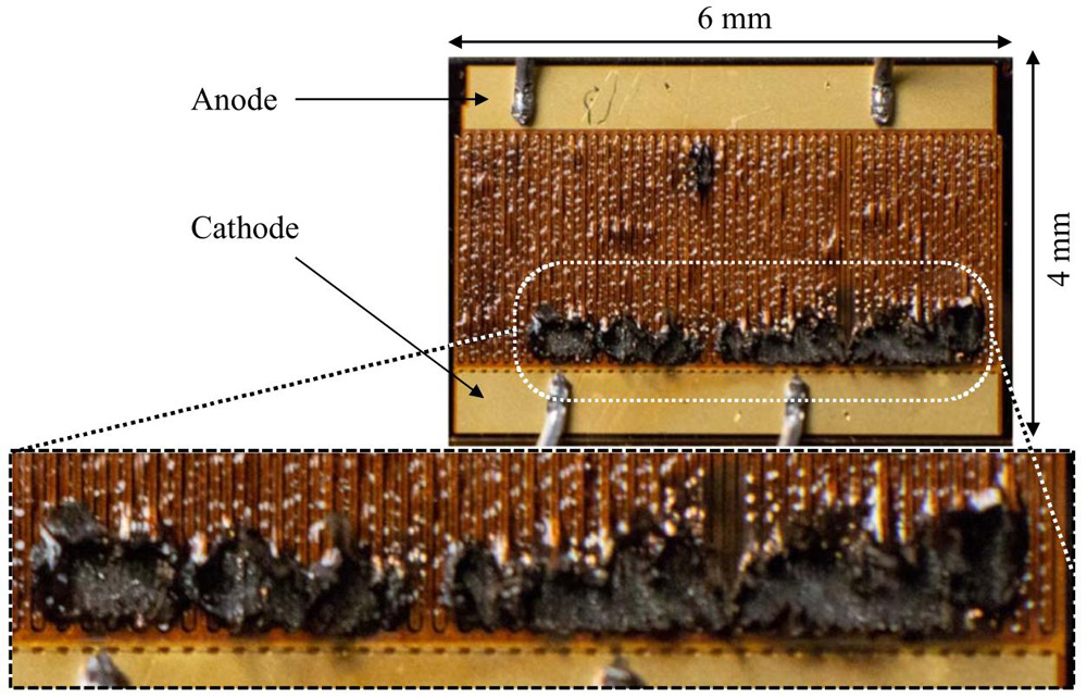
Figure 3: GaN PSJ diode after failure.
After 60A surge failure (Figure 3), the anode fingers showed black burnt out failure points uniformly across the device near the cathode terminal. The researchers comment: “The possible reason for this can be attributed to the triggering/activation of the p-GaN contact near the anode region where the damage can be seen. The activation of the p-GaN region results in a significant number of high-energy minority carriers to be injected into the device, which could result in lattice damage and device failure.
Polarization superjunction diodes GaN AlGaN
The author Mike Cooke is a freelance technology journalist who has worked in the semiconductor and advanced technology sectors since 1997.


