News: Suppliers
26 January 2023
Aixtron launching G10-AsP system at Photonic West
Deposition equipment maker Aixtron SE of Herzogenrath, near Aachen, Germany is launching what it says is the first fully automated AsP (arsenide–phosphide) platform on the market, enabling robust high-volume production linked to very complex requirements. The new system G10-AsP specifically addresses the growing demands in the micro-LED and laser device sectors.
“Micro-LEDs will revolutionize the world of displays as they offer better durability, higher lifetime, a better picture quality and a very low energy consumption. However, this innovative technology challenges the production process as it requires lowest defect levels and highest uniformity rates,” says CEO & president Dr Felix Grawert. “The new system enables the highest throughput of its class with uniformity and defect levels never seen before.”
For the first time, true mass production of micro-LEDs with the most tightened material requirements and reduced chip sizes of 10μm and lower is becoming a reality, says Aixtron. The G10-AsP also meets the complex requirements to produce indium phosphide (InP) laser and VCSELs (vertical-cavity surface-emitting lasers) in high volume.
The new platform G10-AsP will officially be launched on 1 February during the Photonic West 2023 exhibition in San Francisco, CA, USA, where Aixtron will present the new system, explaining the innovations that in the new platform and how it will provide what is claimed to be the highest throughput of its class and maximize cleanroom utilization.
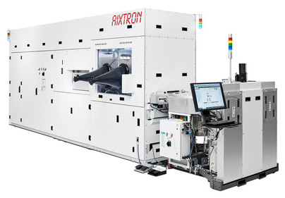
 Picture: Aixtron’s new fully automated AIX G10-AsP system.
The G10-AsP is reckoned to be the largest 200mm AsP batch reactor on the market and comes with in-situ cleaning and automated cassette-to-cassette (C2C) wafer loading. For the first time, the front-end can be equipped with SMIF (Standard Mechanical Interface) pods to further minimize exposure of the epitaxial wafers to the room environment. With in-situ cleaning built-in, users can reset the chamber conditions on demand – either after each process run for the most demanding requirements or just after a production campaign to benefit from highest throughputs. The platform is based on Planetary Reactor technology, which combines the multi-wafer batch reactor concept with single-wafer rotation for the highest wafer uniformity.
Micro-LEDs will not only be used for the next generation of TV displays but also for future smartwatches, smartphones, augmented reality (AR) projection or automotive displays. Analysts expect this area to be the largest market for LEDs in the next 5–10 years.
The one big challenge to reaching the next level for not only advanced micro-LEDs but also InP and VCSEL applications remains uniformity. Optimized on-wafer uniformity and wafer-to-wafer uniformity must be accomplished in a high-volume production process. The new G10-AsP is said to set a new standard with respect to these values, offering a two-to-threefold improvement compared with its predecessor. It is hence reckoned that this fully automated platform will initiate a new era for producing micro-LED and photonic devices, overcoming major obstacles that previously have prevented robust mass production.
In telecoms, photonic devices such as infrared lasers and detectors have laid the foundation for managing the ever-growing data volumes linked to continuously higher bandwidth requirements. Also, they enable 3D sensing (e.g. for facial recognition) and advanced technologies for autonomous driving: With the continuous evolution of this technology, beams must map larger and wider areas. This calls for tighter wavelength tolerances, which translates into very tight requirements for epitaxial layer deposition. Aixtron says that the new G10-AsP can address this need by providing significantly refined control of the epitaxial process with improved material accuracy, reduced defect levels and, as a result, higher yield and better uniformity.
In the production of micro-LEDs, improved uniformity is a prerequisite for economically viable mass production: micro-LED displays rely on a special stamp or matrix transfer process where thousands of LED chips (arrays) of just a few microns in size are picked up and transferred. Because entire arrays of pixels are transferred from the epiwafer substrate, almost perfect uniformity is required – to avoid, for example, a smartwatch or smartphone display having a different color in one corner than the other.


