


News: Optoelectronics
12 January 2023
Amorphous p-NiO/n-Ga2O3 crystal solar-blind detection
University of Science and Technology of China (USTC) claims record detectivity and open-circuit voltage for its nickel oxide/gallium oxide (NiO/Ga2O3) heterojunction solar-blind photodetector (SBPD) [Mengfan Ding et al, IEEE Electron Device Letters, published online 8 December 2022].
Such compact devices are of interest for high-performance, portable, low-power solar-blind ultraviolet (UV) detection systems for secure communication and flame detection, among other applications. Ga2O3 has an ultrawide bandgap in the range 4.7-5.3eV (264-234nm photon wavelength). The bandgap is well away from the visible range 1.65-3.26eV (750-380nm).
The researchers used the NiO/Ga2O3 heterojunction combination to produce a p-n junction due to the difficulty in achieving p-type conductivity in Ga2O3. Amorphous p-NiO has a relatively high hole mobility. The researchers demonstrate that “amorphous p-NiO has potential to construct an excellent staggered band alignment and superior interface with crystalline Ga2O3,” avoiding carrier-blocking trap states.
The substrate for the device (Figure 1) was β-Ga2O3 with a 1μm halide vapor phase epitaxy (HVPE) epitaxial layer with electron (n) concentration of 2x10¹⁶/cm3. The backside ohmic electrode of titanium/aluminium/nickel/gold (Ti/Al/Ni/Au) was applied and annealed after some dry etching. Surface damage from these processes was repaired using a Piranha solution consisting of 2:1 sulfuric acid:hydrogen peroxide (H2SO4:H2O2). This produced “an atomically flat Ga2O3 upper surface with clear step structure and low roughness (0.19nm),” according to the team.
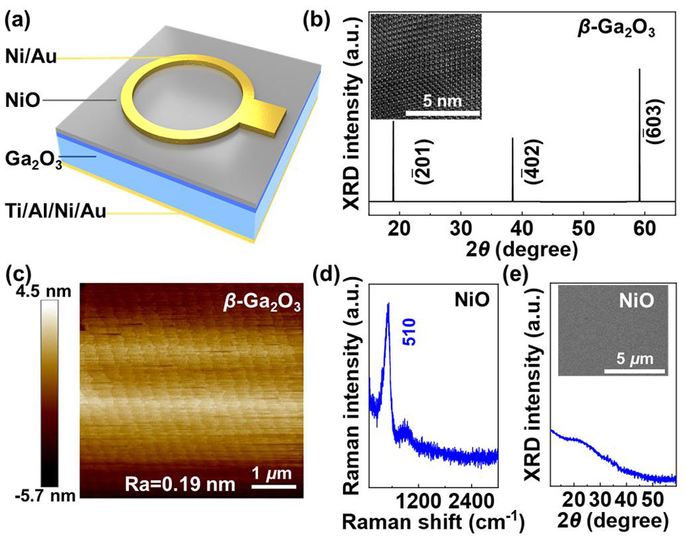
Figure 1: (a) Device schematic diagram. (b) X-ray diffraction (XRD) pattern and transmission electron microscope (TEM) images (inset) and (c) atomic force microscope (AFM) image of β-Ga2O3 single crystal. (d) Raman spectrum and (e) XRD pattern and scanning EM (SEM) image (inset) of amorphous NiO film.
The p-type amorphous NiO was the result of room temperature RF sputtering. The Ni/Au top ohmic ring electrode was applied using electron-beam evaporation. The illumination window area was 1.2x10⁻³/cm2.
The rectifying on/off dark current ratio of the diode between +3V and -3V was 104. The use of NiO, rather than directly applying Ni to the Ga2O3 to form a Schottky junction, enhanced the reverse-bias response to 254nm radiation by four orders of magnitude.
The researchers investigated the performance with varied NiO oxygen content and thickness. The team comments: “The device with 30nm NiO film has the best performance due to the balance of NiO film transmittance and depletion region width of device.” It was also found that higher oxygen content gave better performance, “mainly due to the higher hole concentration”.
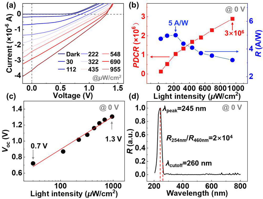
Figure 2: (a) NiO/Ga2O3 heterojunction photodetector current-voltage performance under 254nm illumination with different intensities. (b) Dependence of PDCR and R at 0V on light intensity. (c) Voc as function of light intensity. (d) Normalized spectral response at 0V.
The 0V response to UV is of particular interest since it enables self-powered setups (Figure 2). The dark current noise was at the picoamp scale.
The photo-dark current ratio (PDCR) reached 3x10⁶ under a 254nm illumination intensity of 955μW/cm2 with approximately linear performance. At the same intensity, the open-circuit voltage (Voc) reached 1.3V, “exceeding almost all the reported Ga2O3 heterojunction photodetectors,” according to the team (Figure 3).
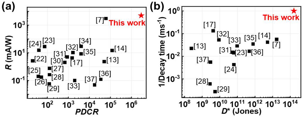
Figure 3: Benchmark plots of (a) PDCR versus R and (b) D* versus 1/(Decay time) from representative self-powered Ga2O3 SBPDs. Red star represents USTC work.
The responsivity peaked at an “ultrahigh” 5A/W at 222μW/cm2, where the specific detectivity (D*) was 1/6x1014 Jones. The spectral performance of R peaked at 245nm, with a cut-off around 260nm. The rejection ratio of 460nm visible light was 2x10⁴. The response time to changes in intensity was better than 1ms.
Nickel oxide gallium oxide heterojunction solar-blind photodetector HVPE
The author Mike Cooke is a freelance technology journalist who has worked in the semiconductor and advanced technology sectors since 1997.


