News: Suppliers
17 July 2023
Applied Materials and Fraunhofer IPMS to create European metrology technology hub
Process equipment maker Applied Materials Inc of Santa Clara, CA, USA and the Fraunhofer Institute for Photonic Microsystems (FhG IPMS) in Dresden, Germany are collaborating to create what is reckoned will be Europe’s largest technology hub for semiconductor metrology and process analysis, aiming to accelerate research and enhance development projects with chipmakers and ecosystem partners across Europe, particularly in the ICAPS (Internet of things, Communications, Automotive, Power and Sensors) market segments.
To be located at Fraunhofer IPMS’ Center Nanoelectronic Technologies (CNT) — which offers applied research on 300mm wafers for microchip producers, suppliers, equipment manufacturers and R&D partners — the technology hub is situated in the heart of Silicon Saxony, Europe’s largest semiconductor cluster. The hub will be equipped with Applied Materials’ eBeam metrology equipment, including its VeritySEM CD-SEM (critical dimension scanning electron microscope) systems, and staffed by Applied engineers and R&D experts.

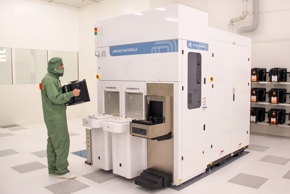
Picture: Applied Materials’ eBeam metrology equipment in the cleanroom at Fraunhofer IPMS.
“Fraunhofer IPMS and its partners will benefit from access to Applied’s industry-leading eBeam metrology systems,” comments Dr Benjamin Uhlig-Lilienthal, head of Fraunhofer IPMS’ Next Generation Computing business unit. “The new technology hub will offer advanced wafer-level metrology in our industrial CMOS environment with Fraunhofer IPMS’s unique ability to loop wafers directly with semiconductor manufacturers,” he adds.
“Our collaborative metrology hub will accelerate learning cycles and the development of new applications for the Fraunhofer Institute, Applied Materials and our customers and partners in Europe,” says James Robson, corporate VP for Applied Materials Europe. “This unique technology hub will have the capability to test and qualify processes on a variety of substrate materials and wafer thicknesses critical to applications across the diverse European semiconductor landscape.”


