News: Optoelectronics
20 July 2023
Silicon-based InAs quantum dot laser operation above 150°C
Institute of Semiconductors and University of Chinese Academy of Sciences in China have claimed record-high continuous wave (CW) operating temperatures of up to 150°C for 1.3 μm wavelength indium arsenide (InAs) quantum dot (QD) lasers directly grown on on-axis silicon (001) substrates [Zunren Lv et al, Optics Express, v31, p24173, 2023]. The devices on silicon (Si) also demonstrated ultra-high thermal stability with effectively constant threshold currents and slope efficiencies over wide temperature ranges.
The team attributes their results to a combination of a low threading dislocation density (TDD) gallium arsenide (GaAs) buffer layers, a high-gain QD active region, and p-type modulation doping.
The researchers comment: “We believe that this work demonstrates the great prospect of Si-based direct epitaxial QD lasers in realizing low power consumption, miniaturization and low-cost silicon photonics chips, which provides a strong driving force for the development of low-cost and high-performance silicon photonic integrated circuits (PICs).”
The team foresees prospects for low cost, low power and high integration of QD laser diodes (LDs) allied with complementary metal-oxide-semiconductor (CMOS) electronic processing units for high-capacity data transmission, high-performance optical computing and high-precision light detection and ranging (LiDAR). Stability of the laser diodes at high temperature is particularly critical when such devices are placed next to heat-generating high-speed CMOS computer processing units (CPUs).
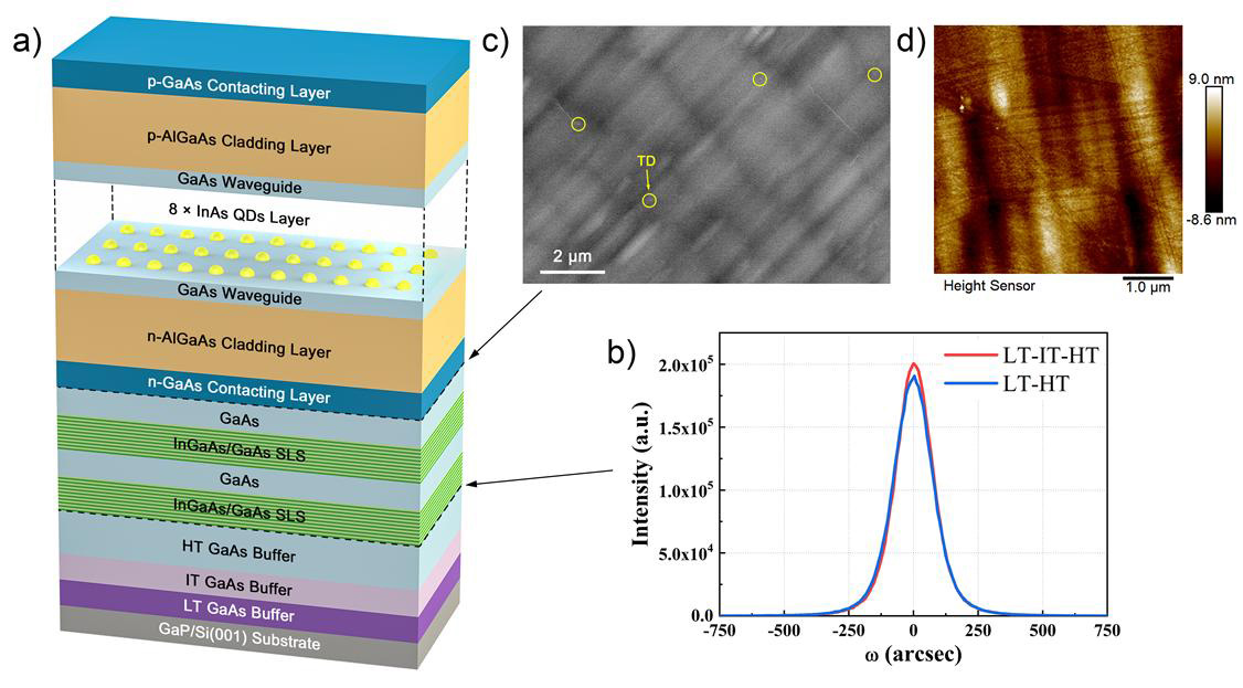
The researchers used molecular beam epitaxy (MBE) on gallium phosphide on silicon (GaP/Si) templates to produce the QD laser materials (Figure 1). The templates were free of anti-phase domains.

Figure 1: (a) InAs/GaAs QD laser epitaxial structure on on-axis Si (001) substrate. (b) Comparison of x-ray rocking curves of 1.6 μm GaAs buffer layers grown by two-step and three-step temperature processes. (c) Electronic channel contrast imaging (ECCI) of 3 μm GaAs buffer interface. (d) Atomic force microscope (AFM) image of 3 μm GaAs buffer interface within 5 μmx5 μm field.
The team took particular care in growing the buffer layers to reduce defect densities in the upper device layers. The first three layers were grown at low (LT, 30nm), intermediate (IT, 70nm), and high (HT, 1500nm) temperatures of 400–500°C, 500–600°C and 600–700°C, respectively. The injection of the IT step reduced the full-width at half-maximum (FWHM) of one x-ray rocking curve to 173.3arcsec, compared with 182.3arcsec for a two-step 100nm LT + 1500nm HT buffer. The threading dislocation density (TDD) was also reduced 10.9% to 1.01x10⁸/cm2 from using the three-step buffer process.
Further measures to promote dislocation annihilation included the growth of InGaAs/GaAs strained layer superlattice dislocation filters and cyclic thermal annealing. ECCI analysis gave a TDD of 4.3x10⁶/cm2 for the complete 3 μm GaAs buffer. The root-mean-square surface roughness was 2.46nm, according to AFM.
The active region in the device layers consisted of eight layers of self-assembled InAs/GaAs QDs. The InAs dots in one layer were covered by a 4nm InGaAs strain-reducing layer, and 45nm GaAs. The layers were separated by 6nm p-type modulation-doped barriers. The hole concentration was of order 1x10¹⁸/cm3, or about 14 holes per QD.
The cladding layers were 1.4 μm aluminium gallium arsenide (Al0.4Ga0.6As), suitably doped. The top contact layer consisted of 300nm p-GaAs.
The material was fabricated into ridge-waveguide lasers with titanium/platinum/gold (Ti/Pt/Au) and gold-germanium/nickel/gold (AuGe/Ni/Au) for the p- and n-type electrodes, respectively. Electrical isolation was provided by 350nm silicon dioxide. The material was thinned to 100nm thick and cleaved to give different cavity lengths. One facet was coated with 95% reflective material.
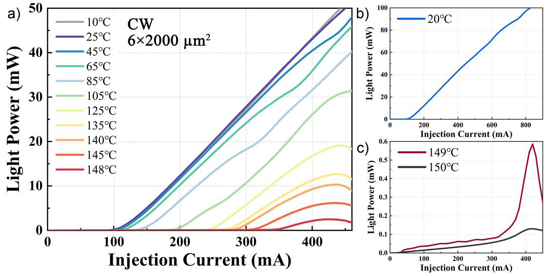
The room-temperature CW threshold current density was 933.3A/cm2 for a 6 μmx1000 μm laser, and 654.9A/cm2 for a wider 30 μmx1500 μm device. The emission wavelength was around 1316nm. The light output power of the wider laser diode reached 91.6mW saturation with a slope efficiency of 0.2W/A. The narrower device had a slightly higher slope efficiency of 0.22W/A, and almost reached 50mW output power.

Figure 2: Temperature-dependent CW power–current curves from 10°C to 150°C for 6 μmx2000 μm QD laser.
A 6 μmx2000 μm device was able to maintain CW lasing up to 150°C with a maximum output of 0.13mW (Figure 2). The researchers comment: “To the best of our knowledge, these results represent the highest O-band CW operating temperatures for any lasers grown directly on silicon substrates including 119°C for offcut silicon and 108°C for on-axis silicon.”
The emission wavelength of this device red-shifted to longer wavelengths at higher temperatures, going from 1313.1nm at 15°C to 1345nm at 85°C. At 125°C and 145°C, the wavelength reached 1375nm and 1377.5nm, respectively.
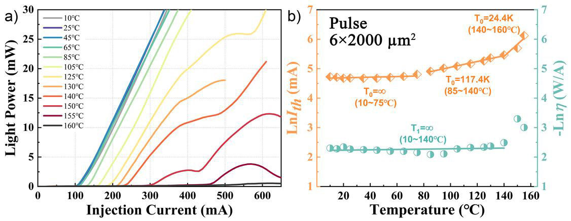
To avoid self-heating effects, the team also studied the lasers under pulsed current injection at different temperatures (Figure 3). For example, at 150°C the 6 μmx2000 μm QD laser had a saturation light output power of 12.3mW, rather than the 0.13mW for CW operation.
The threshold current for pulsed operation was essentially constant over the range 10–75°C, corresponding to an infinite characteristic temperature (T0=∞).

Figure 3: (a) Temperature-dependent pulsed power–current curves from 10°C to 160°C for 6 μmx2000 μm QD laser. (b) Threshold current and slope efficiency versus temperature.
The researchers comment: “This is consistent with the reported highest temperature stability results for GaAs-based QD lasers and is of great value for silicon PICs.”
The characteristic temperature of the slope efficiency degradation with temperature (T1) was infinite, i.e. no degradation, over the wider 10–140°C range.
A wider 10 μmx2000 μm QD laser had more than 25mW output power at 150°C, and 2mW at 160°C, under pulsed injection.
A final variation reported by the team was a reduction in the number of QD layers to five. Comparing the performance of 10 μmx2000 μm devices, the pulsed threshold current density at 25°C for 5-layers was 90A/cm2, a little lower than the 8-layer 99A/cm2 threshold. However, the 5-layer laser diode only reached 120°C before failing to lase. The T0 characteristic was also reduced from infinity for the 8-layer device in the 15–75°C range to 142K for 5 layers.
The team comments: “These results suggest that high-quality multi-layer QDs can significantly enhance the high-temperature performance of Si-based devices.”
The author Mike Cooke is a freelance technology journalist who has worked in the semiconductor and advanced technology sectors since 1997.


