


News: Microelectronics
8 June 2023
AlScN ferroelectric FETs for monolithic 3D NVM integration
Researchers in the USA, Korea and Saudi Arabia report on the performance of field-effect transistors (FETs) using aluminium scandium nitride (AlScN) ferroelectric (FE) to give non-volatile memory (NVM) operation [Kwan-Ho Kim et al, Nature Nanotechnology, published online 22 May 2023].
The team from University of Pennsylvania in the USA, Hanyang University ERICA in South Korea, Pennsylvania State University in the USA, King Abdulaziz University and King Abdullah University of Science and Technology in Saudi Arabia, and University of Tokyo in Japan comment: “The stable memory performance of the FE-FETs, combined with their scalability and low-temperature integration, make a promising case for vertical heterointegration with silicon CMOS logic transistors.”
The researchers see such monolithic three-dimensional (M3D) integration of NVM with complementary metal-oxide-semiconductor (CMOS) logic (‘compute-in-memory’) as overcoming data processing bottlenecks arising from placing the various levels of memory at varying distances with different communication speeds.
The ferroelectric potential of AlScN has only recently been realized, making it an interesting competitor to more established materials such as hafnium zirconium oxide (HZO) with a higher remnant polarization (Pr) of more than 110μC/cm2 and lower processing temperature.
The ferroelectric (FE) transistors (Figure 1) were fabricated on platinum/silicon dioxide/silicon (Pt/SiO2/Si) and aluminium (111)/sapphire (Al/Al2O3) 4-inch templates. The metal template layers were used as back-gates of the transistor, and for controlling the AlScN polarization field. The coercive field (Ec) of the deposited AlScN was −4.5/5.1MV/cm, according to metal–AlScN–metal structural capacitor studies.
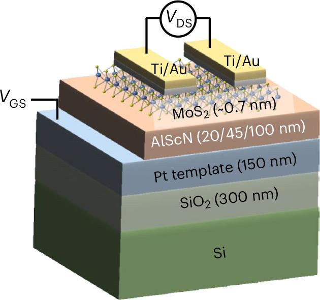
Figure 1: Schematic of MoS2/AlScN FE-FET.
The channel material was the transition-metal dichalcogenide molybdenum disulfide. The researchers comment: “Selecting atomically thin monolayer MoS2 as the FE-FET channel provides a key advantage by exploiting the high Pr of AlScN as an FE gate dielectric because of the ability of MoS2 to support high carrier densities, which is critical for a high ON-current density and high-speed operation as well as alleviating short-channel effects.”
The researchers explain the operation of the devices: “Under a positive (negative) gate voltage above Ec, the FE polarization is switched in the direction pointing towards the channel (opposite of the channel), and consequently, electrons are accumulated (depleted) in the channel, causing a low-threshold-voltage (LVT) (high-threshold-voltage (HVT)) state.”
The AlScN was applied using 150kHz pulsed DC co-sputtering of the metals with nitrogen at 350°C chamber temperature. The relatively low temperature falls within the thermal budget of standard CMOS electronics back-end-of-line (BEOL) processing (usually metal interconnection of the front-end-of-line (FEOL) devices and passivation/insulation). The team was careful to avoid the formation of oxide on the AlScN, which would otherwise seriously degrade the FE-FET performance.
The large-area molybdenum disulfide (MoS2) was deposited as a single layer on two-inch sapphire, using three different chemical vapor deposition (CVD) methods. The Mo was sourced from MoOx or the metal-organic molybdenum hexacarbonyl (Mo(CO)6). The sulfur precursor was variously S powder or hydrogen sulfide (H2S). The MoS2 was then transferred onto the AlScN during transistor fabrication in a wet process.
A 500nm long-channel device on 100nm Al0.68Sc0.32N had a very large memory window (MW) of 18V, along with an ON/OFF current ratio of 107.
The ON-current density at 1V drain bias (VDS) was 71μA/μm. At 3V VDS the ON-current density reached 252μA/μm. The team comments: “To the best of our knowledge, this is among the highest current density values obtained without any channel doping or contact resistance engineering in a 2D channel FET, further highlighting the importance of high-Pr FE materials like AlScN.”
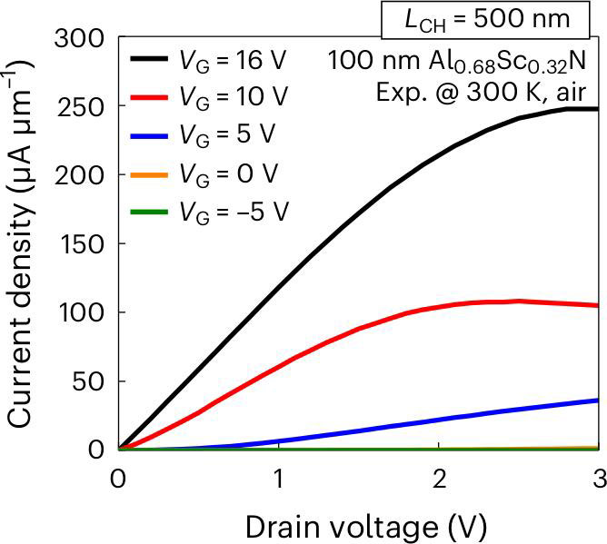
Figure 2: Linear-scale output characteristics of a representative 100nm Al0.68Sc0.32N/MoS2 2 FE-FET at various gate voltages (VG).
The FE switching voltage for the maximum MW could be reduced by thinning the AlScN layer and increasing the Sc content. A smaller switching voltage is needed for low energy consumption and M3D integration of the FE-FETs with Si CMOS. The MW was reduced to 5–6V with a 20nm Al0.68Sc0.32N FE layer.
Aggressive channel length (LCH) scaling down to 78nm with 45nm AlScN FE layer resulted in an 8V MW, and an ON/OFF ratio greater than 106. The team comments that sustaining performance after such aggressive scaling is due to “the high Pr value of AlScN, which noticeably keeps the OFF-current low”.
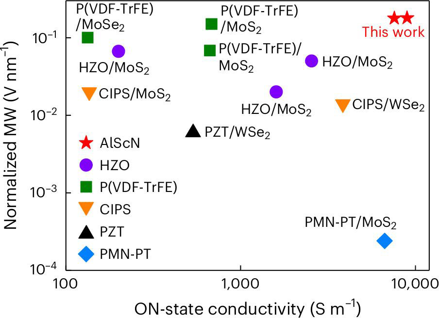
Figure 3: Comparison of normalized MW and ON-state conductivity from reported 2D channel FE-FETs with various FE materials. Left and right red stars correspond to 45nm and 100nm AlScN/MoS2 FE-FETs, respectively.
Comparing the normalized MW and ON conductivity of the long- and short-channel devices with other reports (Figure 3), the researchers comment that their FE-FETs “are among the highest compared with other 2D channel FE-FETs.” They also note the closeness in performance of their long- and short-channel devices (the two stars in the figure).
The programming (PRG) and erasing (ERS) pulses were 500ns/34V and 40ms/12V, respectively. FE materials, such as AlScN, often have a trade-off between pulse width and amplitude.
Retention of the HVT and LVT states of the FE material was extrapolated to have a 10-year scale to maintain a MW of more than 3V. The researchers add: “Aside from time-dependent retention, the devices also exhibit stable switching endurance for more than 10,000 cycles and maintain the ON/OFF ratio when a pulse with 10V amplitude and 40ms width is used.”
Given the large MW, the team also explored AlScN’s potential for multi-bit memory operation for increased effective data density per NVM cell (Figure 4). The researchers comment: “Although the device performance of individual FE-FETs has reached or surpassed floating-gate FETs in flash technology, multi-bit demonstrations in FE-FETs are still in their infancy even for HfOx-based FE-FETs and has never been demonstrated before for nitride FE materials.”
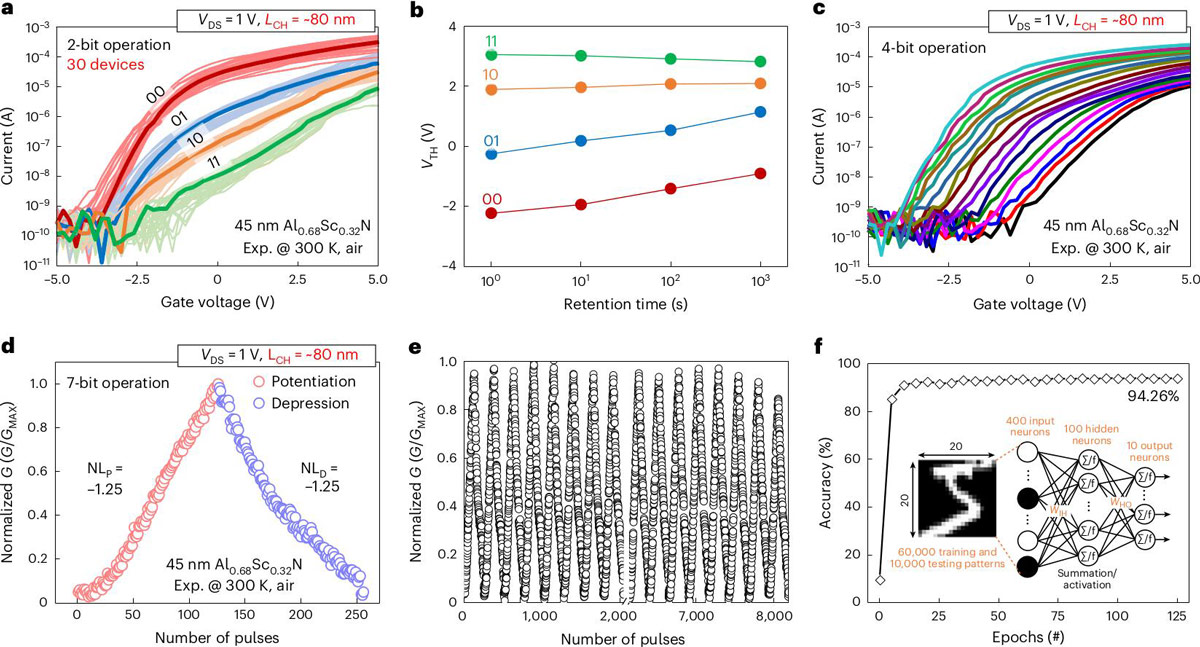
Figure 4: a. Two-bit operation measured from 30 scaled FE-FETs after 10–12V/40ms PRG or ERS pulses. b. Retention of 2-bit VTH states up to 1000s. c. Four-bit operation with 9–12V/40ms pulses. d. Normalized 7-bit LTP/LTD curves obtained from scaled FE-FET. e. Cycle-to-cycle variations of LTP/LTD curve for over 30 cycles (total, over 8000 input pulses). f. Recognition rate as function of the number of training epochs based on the LTP/LTD curve in d, and inset schematic of 400x100x10 MLP-based ANN.
The multi-bit operation was achieved by applying different numbers, widths and amplitudes of pulses to achieve various VTH states. The team comments: “To the best of our knowledge, this is the first demonstration of multi-state programming in FE nitrides and in BEOL-compatible FE-FETs at this scale. These results suggest the foundation for a scalable M3D integration of memory with logic.”
The team also looked at a scheme for using the device as an artificial synapse in a 7-bit operation mode using 15V/150μs 4kHz pulses for long-term potentiation (LTP) and −1 to −15V/150μs for long-term depression (LTD). The corresponding non-linearities (NLP/D) were found to be −1.25.
The device parameters were used in a multi-layer perceptron (MLP)-based artificial neural network (ANN) simulation with 400 input, 100 hidden and 10 output ‘neurons’ connected by artificial synapses.
The researchers report: “The Modified National Institute of Standards and Technology dataset of black-and-white handwritten digit patterns with a size of 20x20 was used for training (60,000) and testing (10,000). As a result, the maximum accuracy based on the LTP/LTD curve reached a very high value of 94.26% (96.19% for software-based simulation).”
The author Mike Cooke is a freelance technology journalist who has worked in the semiconductor and advanced technology sectors since 1997.


