News: Microelectronics
14 June 2023
WIN releases next-gen mmWave E-mode/D-mode GaAs pHEMT technology
WIN Semiconductors Corp of Taoyuan City, Taiwan – which provides pure-play gallium arsenide (GaAs) and gallium nitride (GaN) wafer foundry services for the wireless, infrastructure, and networking markets – has announced the commercial release of its PQG3-0C next-generation integrated millimeter-wave (mmWave) GaAs platform.
Targeting mmWave front ends, the PQG3-0C technology combines individually optimized enhancement-mode (E-mode) low-noise and depletion-mode (D-mode) power pseudomorphic high-electron-mobility transistors (pHEMTs) to enable what is claimed to be best-in-class power amplifier (PA) and low-noise amplifier (LNA) performance on the same chip. The E-mode/D-mode pHEMTs have a threshold frequency (ƒt) of 110GHz and 90GHz respectively, and both employ 0.15µm T-shaped gates fabricated by deep-ultraviolet stepper technology. Deep UV photolithography is a proven, high-volume manufacturing technique for short-gate-length devices and eliminates the throughput constraints of traditional electron-beam patterning. Offering two application-specific mmWave transistors with RF switches and ESD protection diodes, PQG3-0C supports a wide range of front-end functions with increased on-chip functionality.

Both E-mode and D-mode transistors can be used for mmWave amplification and operate at 4V. The D-mode pHEMT targets power amplifiers and provides over 0.6W/mm with 11dB linear gain and close to 50% power-added efficiency (PAE) when measured at 29GHz. The E-mode pHEMT operates best as a single-supply LNA and delivers minimum noise figure below 0.7dB at 30GHz with 8dB associated gain, and third-order output intercept (OIP3) of 26dBm.
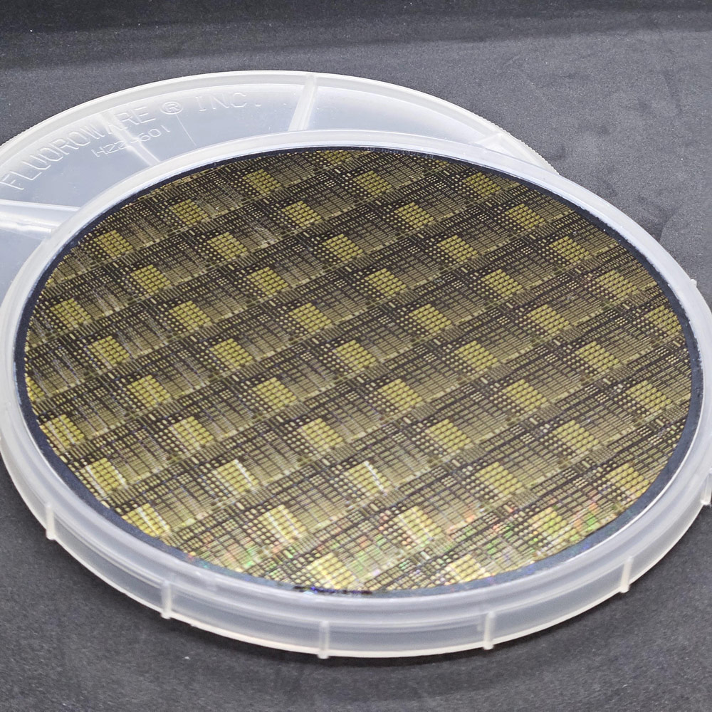
The PQG3-0C platform is manufactured on 150mm GaAs substrates and provides two interconnect metal layers with low-k dielectric crossovers, PN-junction diodes for compact ESD protection circuits, and RF switch transistors. With a final chip thickness of 100µm, a backside groundplane with through-wafer vias (TWV) are standard and can be configured as through-chip RF transitions to eliminate the adverse impact of bond wires at millimeter-wave frequencies. PQG3-0C also supports flip-chip packaging and can be delivered with Cu-pillar bumps fabricated in WIN’s internal bumping line.
WIN is showcasing its compound semiconductor RF and mm-Wave solutions in booth #235 at the 2023 International Microwave Symposium at the San Diego Convention Center, San Diego, CA, USA (11–16 June).


