


News: LEDs
16 March 2023
First transverse DUV-LEDs without n-AlGaN layers
Institute of Semiconductors and Lishui Zhongke Semiconductor Material Co Ltd in China claim the first fabrication of deep-ultraviolet light-emitting diodes (DUV-LEDs) with transverse electron injection from selective-area growth (SAG) n+-type gallium nitride (GaN) [Xingfa Gao et al, ACS Photonics, published online 14 February 2023].
The structure was free from the thick n-type aluminium gallium nitride (n-AlGaN) layer usually used to inject electrons into the LED. The aim was to improve the overall crystal quality of the structure, in particular reducing threading dislocations generated by low-quality n-AlGaN growth that then penetrate the UV-emitting multiple quantum wells, reducing recombination into photons.
The researchers see DUV-LEDs as promising for deployment in sterilization, water purification, UV communication, and in-situ sensing roles. Unfortunately, present external quantum efficiencies (EQEs) are less than 10% for DUV wavelengths less than 300nm.
The AlGaN material was grown on sapphire through metal-organic chemical vapor deposition (MOCVD) in two stages (Figure 1). In the first stage, layers were grown without n-type doping layers: the buffer layers consisted of 3μm AlN, 120nm AlN/AlGaN, 90nm AlGaN superlattice (SL), 20nm undoped grading layer (UGL). High-quality AlN is easier to grown than high-Al-content AlGaN.
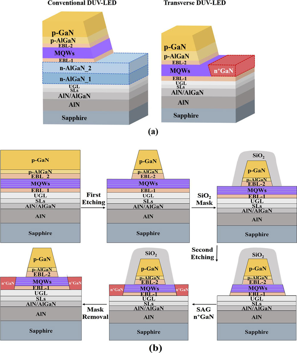
Figure 1: (a) Schematic diagrams of conventional and transverse AlGaN DUV-LED structures and (b) process flow for transverse structure.
The LED layers consisted of a 50nm SL electron-blocking layer (EBL-1), a multiple quantum well (MQW) active region, 50nm EBL-2, p-AlGaN transit layer, and 300nm p-GaN for hole injection. The EBLs -1 and -2 contained layers with 78%/80% and 75%/78% Al, respectively. The MQW had four 2nm Al0.64Ga0.36N wells separated by 15nm Al0.72Ga0.28N barriers.
By not having to grow the n-AlGaN layers, the total growth time was reduced by 3 hours.
The transverse device fabrication consisted of etching a mesa down to the MQW. The mesa was then covered with plasma-enhanced CVD (PECVD) silicon dioxide (SiO2) as a mask for the second-stage MOCVD: selective-area growth (SAG) of n+-GaN. The SAG region was opened with more etching through the MQW and EBL-1.
The two-stage etch process was designed to avoid short-circuiting between the electron and hole injection regions, ensuring current flow through the MQW for the emission of UV light.
After deposition of the n-AlGaN, the SiO2 was removed from the mesa through buffered oxide etching (BOE). The n- and p-type electrodes consisted of annealed titanium/aluminium/titanium/gold and nickel/gold, respectively. The structure was finally passivated with SiO2 and aluminium/titanium/gold deposited for contact pads and a mirror to direct the generated UV through the sapphire backside for collection.
The researchers performed a range of analyses showing reduced dislocations in the transverse LED structure, relative to a more conventional one with n-AlGaN grown before/underneath the MQW and p-type layers. The conventional n-AlGaN was grown in two steps to reduce dislocation generation: 870nm with 78% Al-content, and then 990nm 70% Al. As one indication of reduced dislocation density in the transverse structure, surface roughness was reduced to 0.5nm, compared with 1.28nm for the conventional structure, according to atomic force microscopy (AFM).
Photoluminescence (PL) measurements indicated an internal quantum efficiency (IQE) of 95% for the transverse structure, compared with 48% for the conventional set up. The p-GaN layer was removed for the PL measurements since it strongly absorbs deep UV light. The emission wavelength peaks from the MQWs were 250nm (transverse) and 255nm (conventional) with full-widths at half-maximum (FWHM) of 7.37nm and 8.53nm, respectively.
The two devices had similar current-voltage behavior under forward bias, but leakage was much reduced, and relatively flat, in the transverse structure under reverse bias. The turn-on voltage was around 5V.
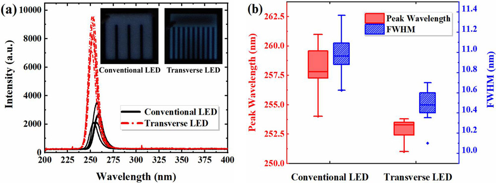
Figure 2: (a) EL spectra and optical microscope images of blue-light from p-GaN layers excited by DUV emissions from conventional and transverse LEDs under 100mA at room temperature. (b) Peak wavelength and FWHM distributions of EL spectra of LEDs.
The electroluminescence from the devices (Figure 2) was much higher in the transverse LED, more than twice that of the conventional structure. The operating voltages were 6.1V and 9.5V for the transverse and conventional LEDs, respectively. A lower operating voltage to supply a given injection current indicates more efficient operation.
The researchers comment: “The absolute EQE and wall-plug efficiency (WPE) values of packaged conventional LEDs operating at 100mA are about 3.2% and 2.6%, respectively.”
Although the LEDs were unpackaged, the team infers from the intensity measurements much higher EQE of the transverse LEDs, adding: “The WPE of the transverse LEDs may be slightly higher than that of the conventional LEDs due to the compromise between EQE and voltage.”
The researchers give two main reasons for the improved performance of the transverse structure: reduced dislocations and reduced DUV absorption due to the absence of underlying n-AlGaN layers.The longer wavelength and broader peaks of the conventional LEDs was suggested to be due to “compositional inhomogeneity and/or compositional fluctuations”.
The author Mike Cooke is a freelance technology journalist who has worked in the semiconductor and advanced technology sectors since 1997.


