News: Microelectronics
23 March 2023
ROHM’s ultra-high-speed control IC technology maximizes performance of GaN switching devices
Due to their superior high-speed switching characteristics the adoption of GaN devices has expanded in recent years. However, the speed of control ICs (for directing the driving of these devices) has become challenging.
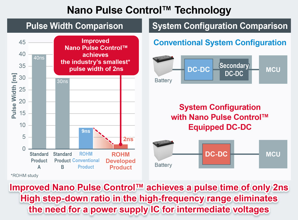
In response, Japan-based power semiconductor maker ROHM Co Ltd has further evolved its ultra-high-speed Nano Pulse Control technology (which is designed for power supply ICs), improving the control pulse width from the conventional 9ns to what is claimed to be an industry-best of 2ns. Leveraging this technology allowed ROHM to establish its ultra-high-speed Control IC technology, which can maximize the performance of GaN devices.
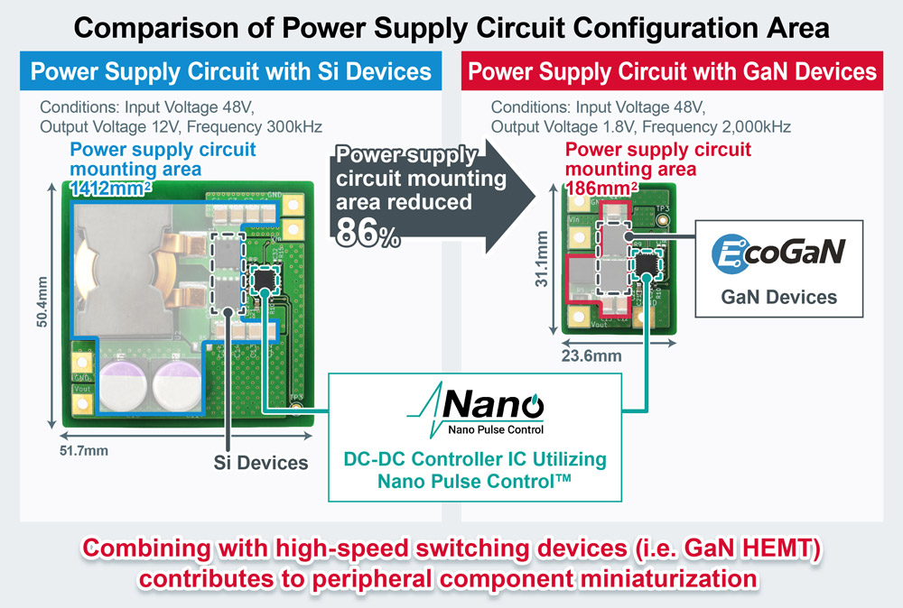
Miniaturizing the power supply circuit requires a reduction in the size of the peripheral components through high-speed switching, says ROHM. Achieving this requires a control IC that can take advantage of the drive performance of high-speed switching devices such as GaN.
To propose solutions that include peripheral components, ROHM established ultra-high-speed Control IC technology optimized for GaN devices utilizing proprietary Nano Pulse Control analog power supply technology. ROHM’s ultra-high-speed pulse control technology achieves a switch-ON time (control width of the power supply IC) on the order of nanoseconds, making it possible to convert from high to low voltages using a single IC — unlike conventional solutions requiring two power supply ICs.
ROHM is working to commercialize Control ICs utilizing this technology, with plans to start sample shipment of 100V one-channel DC-DC Control IC in second-half 2023. Its use, in conjunction with ROHM’s EcoGaN series of GaN devices, is expected to result in significant energy savings and miniaturization in a variety of applications, including base stations, data centers, FA (factory automation) equipment, and drones (Figure 1).

“GaN has been highly anticipated for many years as a power semiconductor material that can achieve energy savings, but there are obstacles such as quality and cost,” notes professor Yusuke Mori, Graduate School of Engineering, Osaka University. “Under these circumstances, ROHM has established a mass-production system for GaN devices that deliver improved reliability while also developing Control ICs that can maximize their performance. This represents a huge step towards the widespread adoption of GaN devices,” he adds. “I hope to contribute to achieving a decarbonized society by collaborating our GaN-on-GaN wafer technology.”
Control IC technology
ROHM says that the Nano Pulse Control technology in its new Control IC has been cultivated by utilizing its vertically integrated production system to combine advanced analog expertise spanning circuit design, processes and layout. Using a unique circuit configuration to significantly reduce the minimum control pulse width of the Control IC from the conventional 9ns to 2ns makes it possible to step down from high voltages (up to 60V) to low voltages (down to 0.6V) with a single power supply IC in 24V and 48V applications. Also, support for smaller drive peripheral components for high-frequency switching of GaN devices shrinks mounting area by about 86% compared with conventional solutions when paired with an EcoGaN power supply circuit (see Figures 2 and 3).


