


News: LEDs
9 March 2023
MOVPE core–shell AlGaN nanorods for UV emission
Researchers based in the UK and Germany report progress in improving the optoelectronic behavior of core–shell aluminium gallium nitride (AlGaN) nanorods as a basis for ultraviolet (UV) light-emitting devices [Douglas Cameron et al, Nano Letters, v23, p1451, 2023].
The team from University of Strathclyde, University of Bath and University of Cambridge in the UK and Technische Universität Berlin in Germany comment: “Our ’GaN-free’ designs upon sapphire substrates prevent self-absorption from lower-bandgap materials. These effectively transparent device structures could additionally allow for backside light extraction, simplifying future contacting schemes in a commercial device.”
In planar devices, UV-absorbing GaN layers are used in p-type layers because of poor doping effectiveness of magnesium in AlGaN. It is hoped that, by using the three-dimensional structuring of nanorods, UV devices will benefit from enhanced doping, reduced dislocation density, and improved light-extraction efficiency.
Also, nanorods tend to be more strain-relaxed, reducing charge-polarization-induced electric fields, and hence the impact of the quantum-confined Stark effect (QCSE) on carrier recombination into photons. Further, the radial deposition of shell layers tends to result in non-polar and semi-polar facets, with reduced or zero electric fields, and thus reduced QCSE.
The researchers used a commercially scalable hybrid top-down/bottom-up method to create a simple single quantum well shell, using metal-organic vapor phase epitaxy (M0VPE) rather than the more laborious molecular beam epitaxy (MBE). The team comments: “As techniques mature, we envisage the addition of electron-blocking layers, multi-quantum well (MQW) structures, and other advancements found to improve conventional LED performance. We expect that the nano-structuring of AlGaN-based LEDs will be key to overcoming the current barriers to efficient deep UV emission in solid-state devices.”
Potential applications for efficient compact UV emitters include water purification, skin-safe disinfection, and resin curing.
The nanorod cores were wet etched out of a 3μm n-Al0.76Ga0.24N layer on AlN/sapphire template, grown by M0VPE.
The team previously reported a similar shell-core structure with the core consisting of AlN, but that attempt suffered from low n-type conductivity due to poor silicon doping. The new AlGaN core demonstrated a doping level of 2x10¹⁹/cm3 and a resistivity of 0.04Ω-cm.
The lithography of the metal dot mask for the nanorods used the diffraction-based Talbot effect. The resulting rods were 210nm diameter, and 1.7μm high.
The shell layers (Figure 1) were also grown by MOVPE: AlGaN to give semi-polar and non-polar facets, and to recover from etch surface damage; a thick quantum well; and p-AlGaN hole injection layer. The quantum well was designed to have a narrower bandgap energy relative to other materials in the LEDs, avoiding absorption of the generated UV light.
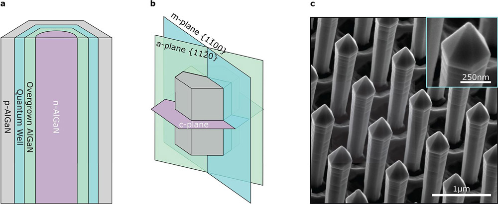
Figure 1: (a) Schematic of core−shell structures (not to scale). (b) Important crystal planes relating to rods. (c) Scanning electron micrograph (SEM) of nanorod array with higher-magnification inset.
Material studies found significant compositional variations, which the team attributes to knock-on effects of the nanorod n-AlGaN core etch.
The structures were subjected to electron-beam excitation to spectrally analyze the cathodoluminescence (CL) at cryogenic temperatures.
The bare etched cores had a main peak at 243nm, and a “very low” longer-wavelength bump centered at 392nm. The short wavelength was attributed to band-edge emissions, while the longer wavelength was associated with defects.
The team comments: “The optical quality of this core is a significant improvement over the AlN core previously employed to create AlN/AlGaN core−shell structures.”
Faceting significantly increased the luminescence in the long-wavelength 360–470nm region, indicating the generation of large numbers of point defects. “These defect bands are ascribed to cation vacancy complexes and are commonly seen in AlGaN alloys,” the researchers comment. This layer didn’t seem to add any extra band-emission peak, probably “due to the close compositional match to the core, combined with the increased defect population”.
The full core-shell structure did have an extra peak from the quantum well around 300nm, varying by about 10nm. The team comments: “Shorter-wavelength emission should be possible using our methods by modifying the quantum well compositions and/or thicknesses.”
Time-resolved CL at 80K gave a very short 19ps lifetime for the carriers in the quantum wells in the m-plane regions. The researchers explain: “Such short lifetimes can only be explained by the absence of or significant reduction in the internal electric fields.” They add: “These short lifetimes are desirable for fast-switching devices and may also help to reduce the influence of droop by keeping carrier densities tolerable, allowing for higher optical powers to be extracted.”
Two schemes were set up for studying the optoelectronic behavior (Figure 2), differing in the nature of the p-contact: a single rod contact of electron-beam-deposited platinum (Pt) on the tip; and, a cleaved block contact, where the space between a small array of rods was filled with Pt from Ga-beam deposition and cut by focused ion-beam (FIB) in the c-plane below the pyramid tip. The n-contact was formed by FIB milling into the n-AlGaN and depositing platinum.
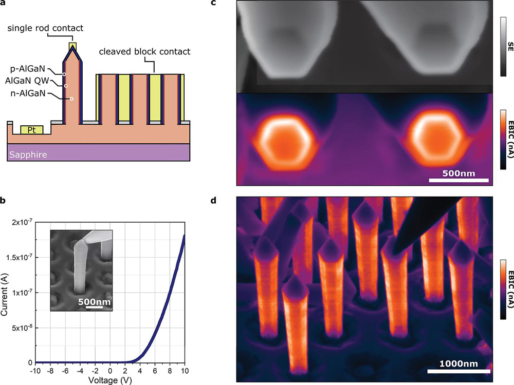
Figure 2: (a) Schematic of nanorod electrical testing architecture. (b) Example current–voltage curve for single rod contacted with nanoprobe as inset. (c) SEM (grayscale) and electron-beam-induced current (EBIC) images of cleaved block contact viewed above. (d) EBIC image of single-rod contact, with nanoprobe contacting above.
The turn-on voltage of the p–n junctions was around 4.5V, “indicating high doping efficiency”. The rectifying ratio between +5 and –5V was 105.
The author Mike Cooke is a freelance technology journalist who has worked in the semiconductor and advanced technology sectors since 1997.


