


News: Optoelectronics
25 May 2023
InAs quantum dot lasers on silicon carbide substrate
University of California Santa Barbara in the USA and King Abdullah University of Science and Technology in Saudi Arabia have reported enhanced thermal performance from an indium arsenide (InAs) quantum dot (QD) laser flip-chip bonded on silicon carbide (SiC), compared with silicon or other heterogeneous substrates [Rosalyn Koscica, et al, Optics Letters, v48, p2539, 2023]. The laser diodes take advantage of the higher 4.9W/cm-K thermal conductivity of SiC at 300K, relieving thermal accumulation in the devices. Native gallium arsenide (GaAs) has a thermal conductivity of 0.55W/cm-K, and silicon has a thermal conductivity of 1.3W/cm-K.
Added interest comes from recent work on non-linear and quantum photonics on the SiC platform. The researchers point in particular to work suggesting that distributed feedback (DFB) could lead to direct on-chip control over spin-defect quantum bits (qubits) in SiC-based quantum computers. The team comments: “With an optimized bonding procedure, the SiC platform will enable integration of III–V light sources with more technology-specific applications, such as DFB or comb lasers for telecommunications.”
The team also points to advantages of enhanced thermal management for high-power-density optoelectronic systems combining lasers with high-performance application-specific integrated circuits (ASICs) consuming up to 200W. Laser performance tends to degrade at high temperature, with the threshold current increasing and eventually failing to lase at all.
The researchers used molecular beam epitaxy of varying layers of indium aluminium gallium arsenide (InAlGaAs) on (001) GaAs substrate for the III–V laser material targeting emissions from the center of the O-band (1260–1360nm), i.e. around 1300nm wavelength (Figure 1).
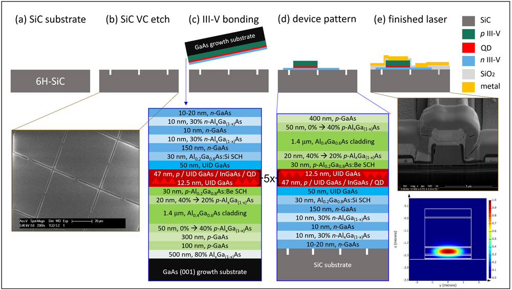
Figure 1: Device processing steps. (a) SiC substrate. (b) Substrate etched with vertical channels (VCs) before bonding, and scanning electron microscopy top view. (c) III–V laser stack epitaxially grown on native GaAs bonded to SiC substrate. (d) Device mesas defined and etched. (e) Cross-sectional schematic, scanning electron micrograph, and simulated normalized intensity profile of optical mode.
The device was fabricated on commercial 2-inch semi-insulating SiC. The substrate was vanadium-doped, giving a resistivity specification of more than 105Ω-cm. The substrate was subjected to reactive-ion etching to create a perpendicular grid of vertical channels at 50μm pitch.
The laser material was flip-chip bonded onto the SiC substrate with a 3nm silicon dioxide interlayer. The structure was annealed at 100°C for 18–24 hours to relieve residual bonding stresses. The resulting III–V laser structure was tensile stressed at room temperature. Gases generated as a result of the bonding process could escape through the VC grid. The GaAs growth substrate and AlGaAs buffer were removed by polishing.
The device mesa fabrication resulted in p- and n-mesas from two dry-etch steps. The n-electrode metals were palladium/germanium/gold/titanium; and for the p-contact was palladium/titanium/gold/palladium/titanium. The n-electrode was passivated with sputtered silicon dioxide before application of the p-contact. The structure was then rapid-thermal annealed at 300°C for a minute before application of another passivation layer, plasma-enhanced chemical vapor deposition (PECVD) silicon dioxide. Titanium/gold was used for the probe contacts. The maximum temperature during device fabrication was 300°C, avoiding thermally induced strain or cracking of the bonded material.
Variously sized Fabry–Perot laser bars were diced and polished from the fabricated material. The emission facets were as-etched with no coatings applied. The lowest threshold current density under continuous wave (CW) operation at 20°C was 233A/cm2. The maximum output power reached 20mW.
A 2500μmx3μm device achieved a wall-plug efficiency of 0.4% at 200mA injection (Figure 2). Above 105°C the lasing mode disappeared. InAs QD lasers on native GaAs substrate have reached 220°C laser operation and 170K characteristic temperature.
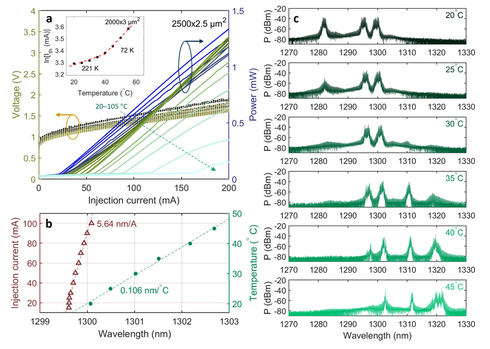
Figure 2: (a) Light–current–voltage (LIV) CW characteristics at stage temperatures from 20°C to 105°C. Inset: determination of 221K T0 characteristic temperature from thermal increase in threshold current between 20°C and 40°C. (b) Thermal and injection current induced spectrum red-shift of ground-state peak in 1500μmx3μm device held at either 20°C constant temperature or 100mA constant injection current. (c) Spectra under varied temperature for device in (b) under 100mA injection.
The researchers comment: “Although the SiC laser maximum temperature is lower, owing to limited optical gain, the higher T0 of 221K indicates reduction in temperature sensitivity compared with native GaAs and non-native silicon substrates.”
For InAs QD lasers on silicon substrates the maximum temperature has reached 110°C and T0 167K. The team expects future work to enhance the performance on SiC substrates, as has been seen in work on silicon substrates.
Spectral analysis showed a ground-state laser peak around 1300nm, and a first excited state around 1295nm. The peaks shifted according to current injection and temperature. At 100mA injection, the thermal red-shift was 0.106nm/°C. At 20°C, the current red-shift was 5.64nm/A.
The author Mike Cooke is a freelance technology journalist who has worked in the semiconductor and advanced technology sectors since 1997.


