News: Suppliers
1 November 2023
Next Level Epitaxy for aluminium nitride thin films
Aluminium nitride (AlN) epitaxial thin films have garnered significant attention due to their exceptional properties, rendering them highly suitable for a wide spectrum of devices such as quantum acoustodynamics, integrated photonics, lithium batteries, LEDs and high-frequency, high-power electronics.
To meet the demands of these applications, the team of experts at Element 3–5 GmbH has pioneered a groundbreaking methodology for the mass production of AlN epitaxial thin films, presenting a substantial leap in the domain of semiconductor fabrication. This innovative method is known as Next Level Epitaxy (NLE). In the context of NLE, a seamless integration of physical vapor deposition (PVD) and chemical vapor deposition (CVD) techniques has enabled epitaxial thin-film growth at surface temperatures below 300°C.
The NLE growth process shares a fundamental resemblance to the thin-film fabrication stages employed in the metal-organic chemical vapor deposition (MOCVD) process. However, in the case of NLE, a distinctive feature emerges as each of the fabrication stages (cleaning, nucleation, and growth) incorporates the use of various plasma sources. Designed, developed and manufactured at Element 3–5 GmbH, these proprietary plasma sources enable processing of 35 x 300mm, 70 x 200mm, 140 x 150mm or 300 x 100mm wafers at each cycle, leading to significant reduction of production costs compared with existing methods.
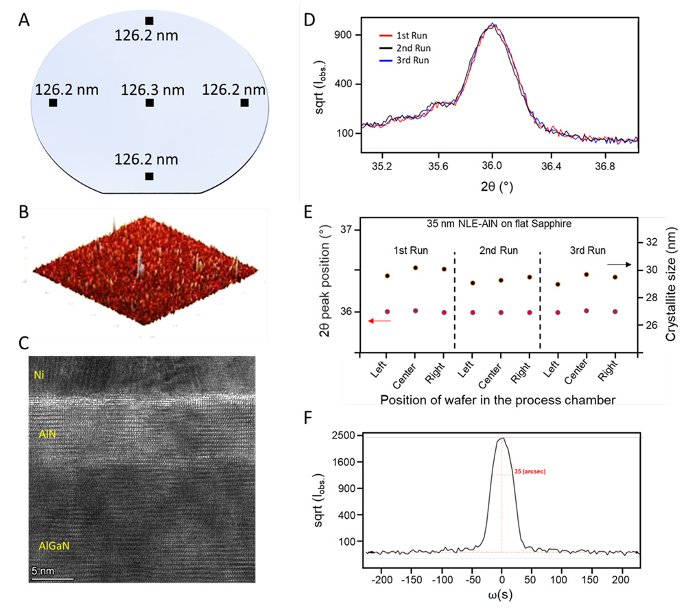
NLE-AlN epitaxial layers exhibit exceptional thickness uniformity over the wafer, a remarkably smooth surface (rms=0.3nm) and a low dislocation density (<107cm–2 within a 45nm AlN layer on sapphire). MOCVD-grown gallium nitride (GaN) on an NLE-AlN-coated flat sapphire wafer exhibits an impressive 002 x-ray rocking curve (XRC) full-width at half-maximum (FWHM) value of 77arcsec, measured within a GaN layer thickness of 2μm. Preserving GaN structural integrity is crucial for forming a vital two-dimensional (2D) electron gas in power transistors. An 8nm NLE-AlN layer on a partly processed high-electron-mobility transistor (HEMT), with mesa isolation and ohmic contacts, displayed a sharp interface and epitaxial growth confirmed by high-resolution transmission electron microscopy (HRTEM) analysis, substantially reducing gate leakage current by three orders of magnitude.

Figure 1: Characterization results of NLE-AlN films: (A) ellipsometry reveals consistent thickness across the entire wafer; (B) atomic force microscopy (AFM) height profile (1μm x 1μm) yields a root-mean-square (rms) value of 0.3nm; (C) HRTEM displays a uniform interface between NLE-AlN and AlGaN; (D) XRD measurement demonstrates a run-to-run reproducibility of the 2θ peak; (E) the 2θ peak position and crystallite size of NLE-AlN remain consistent across all chamber positions; (F) x-ray rocking curve (XRC) analysis reveals a 002 peak FWHM of 35arcsec.
Furthermore, a comparison was conducted between the growth of a light-emitting diode (LED) structure on NLE-AlN on a patterned sapphire substrate (PSS) and the same LED structure using a standard PSS-based process. While the NLE-AlN templates did result in a reduction of the growth time in MOCVD by 2.5 hours, it is noteworthy that the GaN crystal quality remained similar, with the 002 XRC FWHM peak measuring about 200arcsec for both the NLE-AlN templates and the standard templates, despite the NLE-AlN LED being 2μm thinner.
When subjected to photoluminescence analysis, a twofold reduction in standard deviation in intensity was observed for the NLE templates. In the realm of UV-C applications, the deposition of 2µm AlGaN with 60% aluminum content on NLE-AlN yielded XRD FWHM values of 780 / 1070 arcsec for the 002 / 102 plane, whereas annealing a 150 nm NLE-AlN layer improved these values to 50 / 350 arcsec for the 002 / 102 planes.


