News: LEDs
28 September 2023
Germanium–tin MQW LEDs on 12-inch silicon substrate
Researchers based in Singapore, China and the USA claim the first germanium–tin alloy (GeSn) multiple quantum well (MQW) light-emitting diodes (LEDs) on a 300mm (12-inch)-diameter silicon (Si) wafer [Shaoteng Wu et al, Photonics Research, v11, p1606, 2023]. The deployment on the largest-diameter wafers so far increases the potential for mass production and reduces manufacturing costs of complete integrated silicon photonic systems.
Ge and Sn both lie in the group-IV column of the periodic table, like silicon. This makes them potentially easier to integrate with mainstream Si-based electronics. However, these materials are not conducive to light emission, with the narrowest gap between the conduction and valence bands being indirect rather than direct. Some progress has been made in the GeSn alloy system in massaging the band structure so the direct and indirect gaps are more equal, boosting light-emission.
The researchers from Nanyang Technological University in Singapore, Institute of Semiconductors in China, Applied Materials Inc in the USA, and the National University of Singapore see potential for their work in the 2 μm wavelength range (1900–2100nm) with applications in biomedical and gas sensing (especially CO2 sensors), and 3D light detection and ranging (LiDAR). Also, for optical communications, hollow-core photonic bandgap fibers (HC-PBGFs) have recently been found to have a lowest-loss window around 2 μm.
The 300mm (12-inch) GeSn MQW on (001) Si wafers were produced on a commercial reduced-pressure chemical vapor deposition (RPCVD) system. The use of such a system opens the way to large-scale manufacturing.
The MQWs were grown on a 1.2 μm Ge strain-relaxed buffer layer, between 200nm p- and n-type Ge contact layers. The buffer confined defects to near the Ge/Si interface. The wells consisted of 7.5nm Ge0.92Sn0.08 alloy, and the barriers 20nm Ge. The 15-period MQW structure was grown at less than 350°C.
The researchers comment: “The thin GeSn well layers were deliberately designed to provide better carrier confinement for excitons and to inhibit dislocation formation from strain relaxation.”
The GeSn alloy was 0.0116% pseudomorphically strained, according to x-ray analysis.
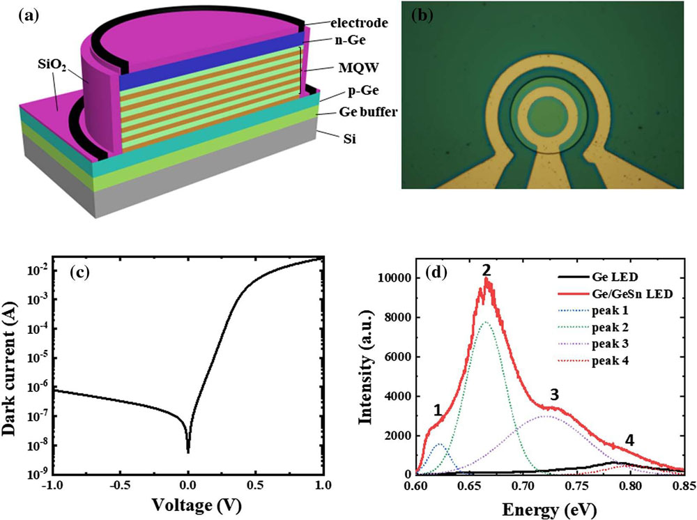
Double-mesa LEDs were fabricated on the 300mm GeSn material (Figure 1). The top mesa was formed through chlorine-based reactive ion etch (RIE) down to the p-Ge contact layer. The bottom mesa electrically isolated the devices by further RIE. The etched surfaces were passivated with 400nm plasma-enhanced CVD (PECVD) silicon dioxide (SiO2). The titanium/gold electrodes were evaporated into windows fluorine-based reactive ion etched into the passivation.

Figure 1: (a) Three-dimensional (3D) schematic of GeSn/Ge MQW LED; (b) top-view microscope image; (c) current−voltage characteristics; (d) room temperature electroluminescence (EL) spectrum, compared with Ge LED.
The resulting devices demonstrated on/off current ratios ~104 for ±1V bias. The ideality factor was 1.36, relatively close to the 1 that is ideal for PN junctions. The dark current was 0.78 μA (27.58mA/cm2) at −1V.
“Due to the low threading dislocation densities (TDDs) from the pseudomorphic growth, the dark current density of our device is one of the lowest of GeSn photodiodes with similar Sn content,” the team reports.
The EL spectrum for the device with 23mA injection showed four emission peaks, according to Gaussian fits. The dominant peak 2 energy was around 0.665eV, corresponding to a 1864nm wavelength. A comparison spectrum for a Ge LED (900nm intrinsic layer) had a peak at 0.785 (1578nm). The red-shift of the GeSn MQW structure was consistent with theoretical 1D Poisson–Schrödinger calculations that gave about 0.660eV as the bandgap for the GeSn MQW.
The researchers comment: “The emission of the GeSn LED covers a wide range from 0.65eV to 0.85eV (1458–2066nm), which covers the S, O, L, U and 2 μm optical communication bands.”
The integrated emissions of the GeSn MQW LED were 27.58x that of the p-i-n Ge LED comparison device. The researchers estimate the energy difference between the indirect L- and direct Γ-valley was reduced to 71.7eV in the GeSn alloy from 134.5eV in Ge. The reduced difference enables more electrons to be thermally excited into the Γ region, boosting the EL intensity exponentially.
The non-dominant peaks 1, 3 (0.723eV/1715nm) and 4 were attributed to the indirect band of the GeSn/Ge structure, the Ge direct band, and “Fabry–Perot modes between Ge-VS/Si and Ge/air interfaces or the Ge peak from the buffer Ge layer”, respectively.
The intensity of the EL emission of the GeSn MQW LED increased approximately linearly between 35A/cm2 and 1768A/cm2. The MQW peak 2 red-shifted only slightly from 0.668eV to 0.664eV over the same current injection range. The Ge direct peak 3 red-shifted more significantly from 0.737eV to 0.718eV. The researchers point to a general view suggesting that EL peaks will red-shift when injection current increases due to Joule heating from electrical excitations. Band filling, widening the effective gap, can counteract this effect, perhaps explaining the minimal shift in peak 2.
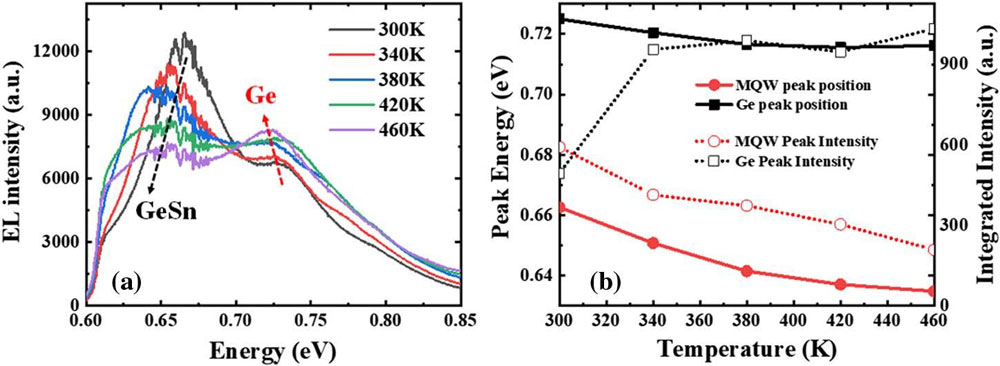
The researchers also investigated the performance at increased ambient temperatures up to 460K (187°C) that would reflect potential thermal conditions for such devices in practical operation (Figure 2). Such temperatures are “higher than the maximum temperature in silicon integrated circuits,” according to the team.

Figure 2: (a) EL spectra as function of temperature at 1900A/cm2; (b) peak position and EL integrated intensity versus temperature.
The bandgaps are expected to shrink at high temperature, resulting in an observed red-shift in the emission peak to lower photon energy. The MQW peak shifted by 27meV between 300K and 460K. The Ge peak is rather less affected.
In terms of measured intensity, the Ge peak increases somewhat, while the GeSn peak declined with increased temperature. Partly this can be explained by the MQW peak 2 moving towards the 0.610eV/2030nm measurement edge of the nitrogen-cooled linear indium gallium arsenide (InGaAs) detector array used to collect spectral data. For the Ge peak, the increased temperature increased the rate of excitation into the direct Γ region of the conduction band profile.
The researchers comment: “Due to the incorporation of Sn, GeSn is closer to direct-bandgap materials, resulting in reduced competition between direct- and indirect-bandgap luminescence. The non-radiative recombination due to the defects from non-equilibrium GeSn growth processes is dominant when the temperature increases. Thus, the method for enhancing the EL intensity of GeSn LEDs from increasing temperature perhaps is unrealistic, as it may occur only on very low Sn content (<4%) GeSn LEDs, which are inefficient.”
GeSn LEDs PECVD Silicon substrate
https://doi.org/10.1364/PRJ.491763
The author Mike Cooke is a freelance technology journalist who has worked in the semiconductor and advanced technology sectors since 1997.


