News: Microelectronics
21 September 2023
Recessing metal contacts for GaN transistors
Researchers based in Sweden report low ohmic contact resistance (Rc) for recessed titanium/aluminium (Ti/Al) metal electrodes with a view to deployment in gallium nitride (GaN) high-electron-mobility transistors (HEMTs) and other transistors [Ding-Yuan Chen et al, Semicond. Sci. Technol., v38, p105006, 2023]. Rc values as low as 0.14Ω-mm were achieved with a low annealing temperature of 550°C.
The team from SweGaN AB, Chalmers University of Technology, Linköping University, Terahertz Materials Analysis Center, and Lund University, comment that their approach “provides a large process window without the requirement of precise control of the recessed etching depth.”
Lowering Rc for HEMTs should reduce power losses, making for less heat and noise generation, while increasing power output and efficiency. The team sees their electron-beam evaporation process as being less complex than other recessed contact structures that regrow doped III–nitride material in metal-organic chemical vapor deposition (MOCVD) in the recess. Electron-beam evaporation is more favored in industrial production.
The researchers comment: “The formation of ohmic contacts requires deposition of ohmic metal stacks (Ti and Al in this work) followed by annealing to extract nitrogen from (Al)GaN, yielding compounds such as TiN, AlN and AlxTiyN. This process hence creates N-vacancies in the (Al)GaN, which act as donor-like dopants, resulting in a n-type region.”
If the annealing temperature is too high (above ~800°C), the aluminium will melt, making smaller-size contacts difficult to manufacture.
The GaN HEMT wafers used in the study were supplied by SweGaN. The material was grown on silicon carbide (SiC) by MOCVD, using SweGaN’s QuanFINE buffer-free structure aimed at telecommunications (satellites, 5G base-stations,...) and high-power (electric vehicles,...) deployment.
“By removing the conventional thick doped buffer layer, we are able to bring the hot channel closer to the heat-sink SiC substrate, eliminate Fe-related deep traps, and shorten the production time,” SweGaN explains on its website.
The HEMT epitaxial material was supplied in two forms: Epi I/II, consisting of 60/60nm AlN nucleation, 260/255m GaN channel, 1.5/1.2nm AlN spacer, 3.3/9.7nm Al0.52Ga0.48N/Al0.3Ga0.7N barrier, and 1.4/2nm GaN cap, respectively. The respective sheet resistances, as measured through eddy currents, were 316 and 298Ω/□.
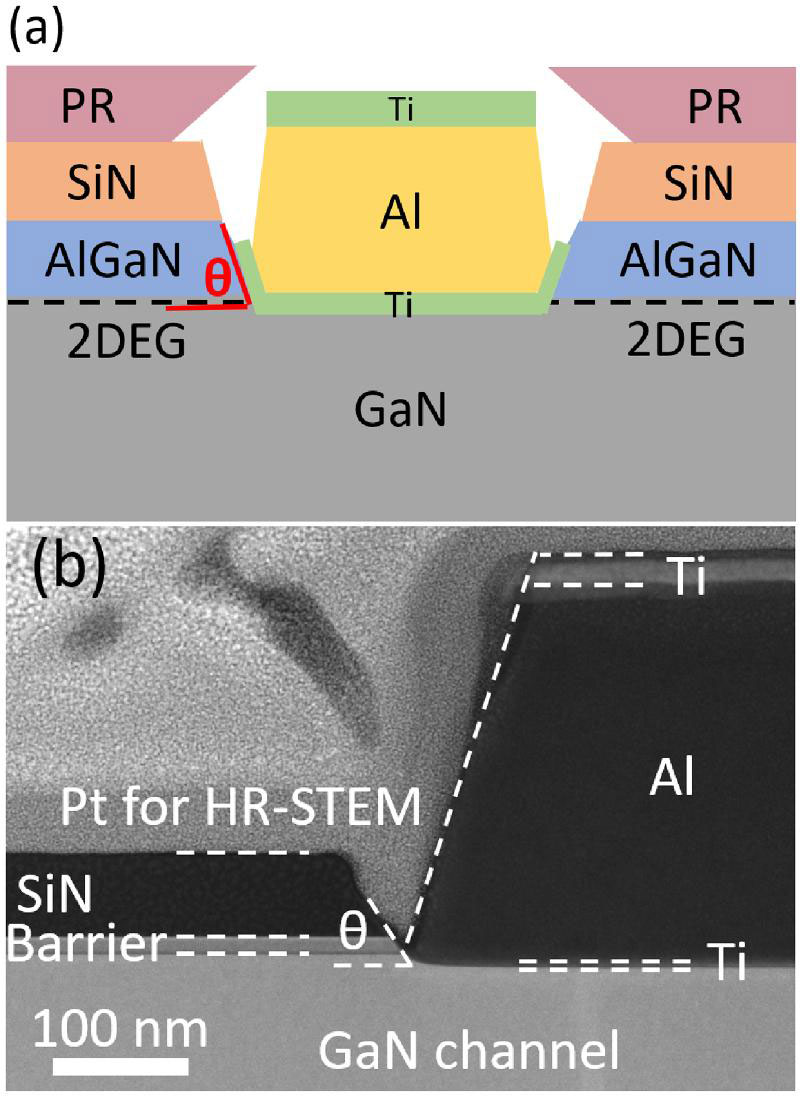
The contact resistance of the proposed channel contact (Figure 1) was evaluated using fabricated transfer length method (TLM) structures on 16mm squares of the HEMT materials. First, silicon nitride (SiN) passivation was applied using low-pressure CVD. Electrical isolation was through mesa etching to ~120nm below the two-dimensional electron gas (2DEG) that constituted the channel.

Figure 1: (a) Schematic of TLM structure. (b) High-resolution scanning transmission electron microscope (HR-STEM) cross-section of annealed TLM with 10°-tilted 3nm tTi on Epi II.
The contact recess sidewall angle, θ, was controlled in turn by the photoresist (PR) profile angle. Key parameters for this were exposure dose, reversal baking temperature, and developing time. The recess for the contact was fabricated by inductively coupled plasma reactive-ion etch (ICP-RIE), using nitrogen trifluoride (NF3) and chlorine (Cl3) gases for removing the SiN and AlGaN/GaN layers, respectively. The recess etching continued to ~12nm below the 2DEG.
Native oxide was removed from the recessed sidewalls with buffered hydrofluoric acid and diluted hydrochloric acid, before electron-beam evaporation of the Ti/Al/Ti metal ohmic contact electrodes. The top Ti layer was 20nm. The other layer thicknesses were varied during the investigations. The width of the contact was 100μm, with the ohmic contact distance in the range 5–30μm.
The researchers comment: “The ohmic recess and the metallization are realized with the same resist, making the ohmic contact self-aligned to the recessed region. The first Ti layer was deposited with a 10° tilt and a low deposition rate of 0.05Â/sec to ensure good sidewall coverage and better thickness control, while the other two layers were deposited without tilt.”

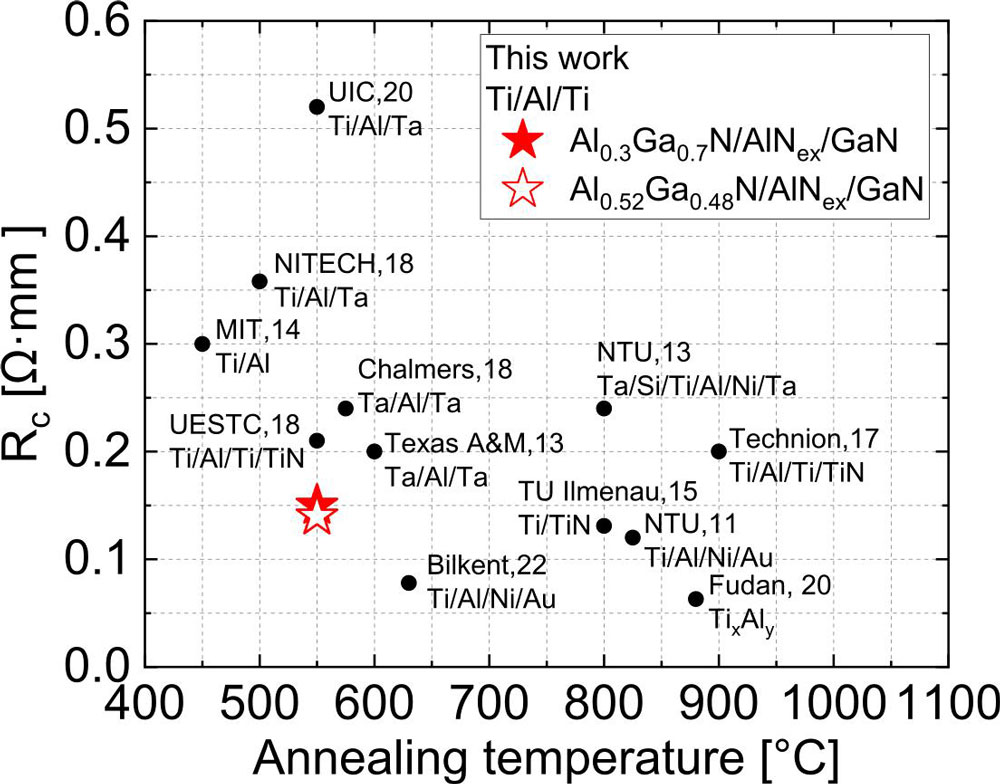
Figure 2: Benchmark of Rc versus annealing temperature on AlxGa1-xN/GaN (x > 0.22) HEMT epi-structures.
The structure was rapid thermal annealed at 550°C in 1 minute cycles until the measured contact resistance (Rc) saturated. Measurements were made with four-point probing.
The lowest Rc for Epi I was 0.14Ω-mm from electrodes with 3nm bottom Ti thickness (tTi) and 280nm Al (Figure 2). The θ angle was ~55°. The contact resistance remained below 0.25Ω-mm with θ in the range 50–60°. A similar electrode on the Epi II material yielded a Rc of 0.15Ω-mm.
The researchers believe that annealing at a slightly higher temperature, but still below the aluminium melting point, could reduce Rc further.
GaN transistors GaN HEMTs MOCVD
The author Mike Cooke is a freelance technology journalist who has worked in the semiconductor and advanced technology sectors since 1997.


