


News: Optoelectronics
25 April 2024
Reconstituted silicon wafers with III-V and Si dies
Imec in Belgium has reported on a fab-compatible indium gallium arsenide on indium phosphide (InGaAs/InP) to silicon (Si) wafer reconstitution (WARE) process [Gauri Karve et al, Jpn. J. Appl. Phys., v63, p04SP42, 2024]. The reported work was carried out on 200mm silicon wafers at Imec’s facility. The team comments: “The method is compatible with the standard CMOS back-end-of-line and extendable to 300mm.”
The researchers see a wide range of potential applications in photonics, RF, imaging, and sensing systems. The team also reports that it has used the technique to realize a micro-fluidic lab-on-chip solution.
The team points out that while compound semiconductors offer superior performance for light generation and RF handling, “high-performance silicon still remains the best candidate for required drivers in silicon photonics, read-out electronics for imagers, and beam-forming chips in RF.”
Co-integration of III-V and silicon should also enable devices to be placed closer together, reducing the effects of parasitic structures, reducing operating power and lowering latency to boost data-handling rates.
First, a ‘pocket wafer’ was constructed from siliicon, using deep etch to create the pockets, followed by backgrinding of the wafer to leave 350-400μm thickness. This thickness was considered adequate for robustness in robot-handling scenarios.
The ‘pockets’ consisted of rectangular through holes in which various III-V/silicon epitaxial dies were placed before transfer and bonding to a final 200/300mm silicon wafer for subsequent processing. The dies could be chosen to be good quality, improving process yields. The pocket wafer was attached with temporary adhesive to a carrier wafer. The use of temporary glue helps to improve dielectric bonding yield and across-wafer uniformity of the reconstituted wafer, the team reports.
The researchers comment: “There are many possible implementations of this basic idea such as different materials for bonding III-V and silicon layers, sequence of processing, etc — each one with their pros and cons. Application-dependent technical specifications and cost constraints primarily drive the integration choices.”
The III-V dies contained a PIN diode epitaxial structure of indium gallium arsenide lattice-matched to the indium phosphide substrate. A thin oxide cap was used to protect the device structure during transfer.
The InGaAs/InP, along with plain silicon and InP dies were singulated using ‘stealth dicing’, apparently referring to Hamamatsu’s laser-based process, for which Hamamatsu Photonics owns the ‘Stealth Dicing’ trademark. Stealth dicing results in smoother sidewalls over mechanical saw processing.
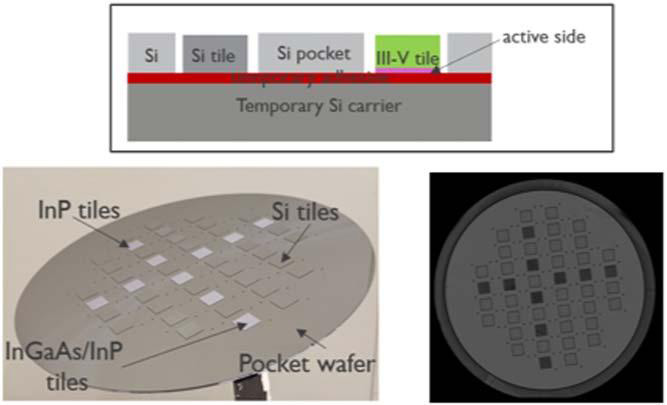
Figure 1: Carrier wafer populated with III-V and silicon tiles: (a) optical and (b) scanning acoustic microscope (SAM) images.
The dies were put in the pockets using a pick-and-place tool — the 1cmx1cm InGaAs/InP dies were inserted active side down (Figure 1). The team reports: “Using stealth dicing for III-V and silicon dies, and a die corner to silicon pocket alignment, a placement accuracy within ±10μm was achieved.”
The researchers add: “The active III-V surface is exposed only at the end of the reconstitution flow, protecting the active side during the reconstitution steps.”
The carrier wafer assembly was passivated with an ultra-thin oxide layer, then edge trimmed, and collectively thinned via grinding. The researchers worked with DISCO USA to optimize the grinding process, resulting in less than 3μm variation in thickness across the wafer.
The dies were bonded to the final silicon wafer using plasma-activated dielectric bonding with the back surface of the dies and pocket wafer being coated with 200mm of thermal oxide (Figure 2). Post-bond annealing was carried out in a dedicated bond chamber with the aim of improving yields over external furnace-based annealing. The temporary carrier was then removed and the adhesive cleaned away in a wet process.
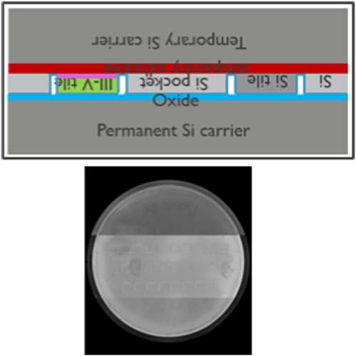
Figure 2: SAM image after dielectric bonding to permanent silicon carrier.
The researchers validated the process by fabricating circular PIN diodes of different radii on InGaAs/InP/Si coupons diced from the 200mm wafer alongside epitaxial InGaAs on InP material. The p- and n-electrodes consisted of non-annealed titanium/palladium/gold.
There was no significant impact of the InGaAs/InP/Si bonding process on diode dark-current performance, relative to the native InGaAs/InP diodes (Figure 3). The effects of sidewall recombination were essentially the same, as shown by the perimeter/area ratio for different radius devices. The ideality factor (n) was about 1.3 for both device species.
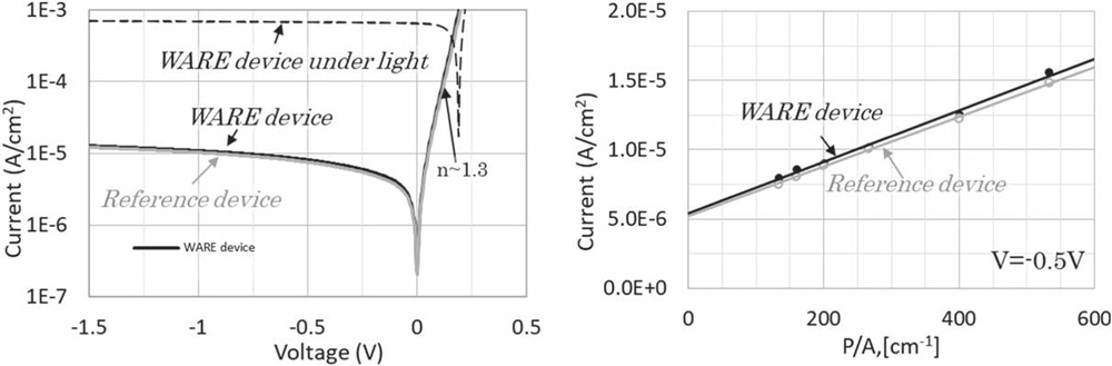
Figure 3: Typical normalized current versus voltage measurements (left) and normalized current versus device perimeter/area ratio (right) for reconstituted (WARE) and as-grown (Reference) devices.
Using temperature variation, the researchers also extracted activation energies at various reverse biases. These results were also the same between the WARE and reference diodes.
The researchers comment: “These observations show that the wafer reconstitution process has no impact on the fabricated device performance.”
Reconstituted silicon wafers InGaAs InP PIN diodes CMOS
https://doi.org/10.35848/1347-4065/ad32e2
The author Mike Cooke is a freelance technology journalist who has worked in the semiconductor and advanced technology sectors since 1997.


