


News: Microelectronics
11 April 2024
HEMTs with 3C-SiC on 4H-SiC interfaces
Japan’s National Institute of Advanced Industrial Science and Technology (NAIST) claims the first fabrication of high-electron-mobility transistors (HEMT) constructed using 3C/4H-polytype crystal heterostructures of silicon carbide (SiC) [Hiroyuki Sazawa et al, Appl. Phys. Lett., v124, p120601, 2024].
A two-dimensional electron gas (2DEG) has previously been found to form on the 3C-SiC side of a heterojunction with 4H-SiC grown with a carbon-face (Figure 1). This is similar to the aluminium gallium nitride (AlGaN) on GaN heterostructure often used as the basis for GaN HEMTs.
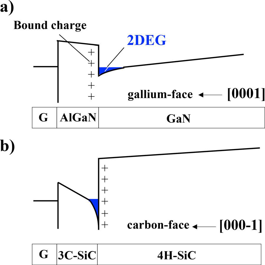
Figure 1: Schematic band diagrams for (a) AlGaN/GaN and (b) C-face 3C-/4H-SiC heterostructures.
The 2DEGs in both cases arise due to the differences in the charge polarization properties of the chemical bonds. For the AlGaN/GaN structure a layer of bound positive charge forms in the AlGaN barrier, attracting a layer of electrons to the GaN side of the interface.
The 3C-SiC/4H-SiC has the bound charge in the 4H-SiC, and the 2DEG on the 3C-SiC side. Also, the 3C-SiC/4H-SiC has a larger conduction band offset of 0.93eV, compared with 0.38eV for Al0.3Ga0.7N/GaN.
The NAIST team sees potential for the 3C/4H-SiC HEMTs for high-power/high-frequency applications in high-power radars, broadband telecommunications, and high-resolution LiDAR. The electron saturation velocity in 3C-SiC can reach 2.5x107cm/s, comparable to the performance of GaN. High saturation velocities are important for increasing frequency performance of amplifiers.
Areas where SiC may have an advantage over GaN-based devices include growth quality and thermal conductivity. The 3C/4H-crystal structures have much smaller lattice and thermal expansion mismatches than AlGaN/GaN, creating potential for higher-quality interfaces. The higher thermal conductivity of SiC is of advantage for management of high power densities in electronic systems.
Further, SiC is more compatible with silicon production processes such as gate oxidation and p-type doping through ion implantation.
The researchers used thermal chemical vapor deposition to create a 24nm 3C-SiC epitaxial layer on 12mmx12mm 4H-SiC substrates (Figure 2). The resistivity of the substrate was >10MΩ-cm.
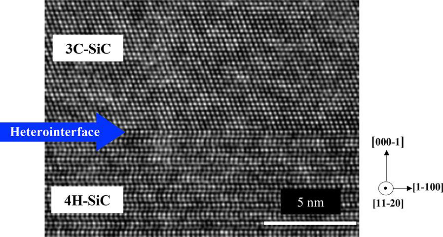
Figure 2: High-resolution transmission electron microscope image of C-face 3C/4H-SiC heterointerface.
Hall measurements found the mobility and sheet carrier density to be 586cm2/V-s and 1.48x10¹³/cm2, respectively. The team reports that it has achieved mobility values up to 780cm2/V-s, about half the value in GaN, in previous work on 3C/4H-SiC structures.
Fabricated HEMTs featured a 200nm-high mesa, annealed nickel source/drain electrodes, and gold gate. The gate length was 10μm and the width 115μm. The gate was separated from the source and drain by equal spaces of 15μm.
The device was normally-on with a maximum drain current of 47.5mA/mm at 7V drain bias at zero gate potential (Figure 3). The extrapolated threshold voltage was −3.8V, although there was gate current leakage throughout the −4–0V gate potential test range. In the –1–0V gate potential range, the transconductance was 13.5mS/mm.
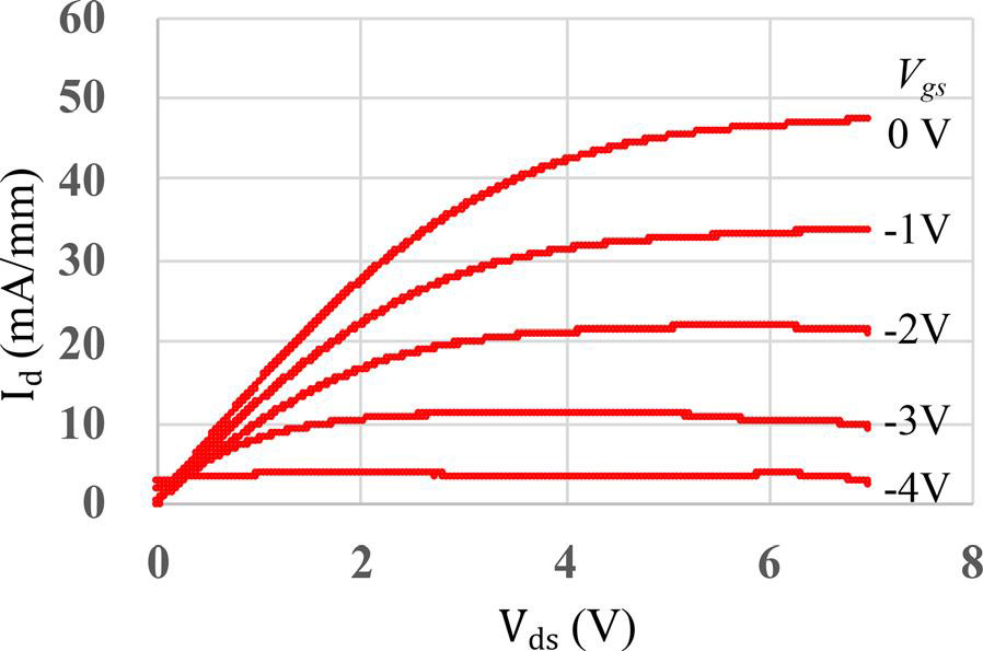
Figure 3: Drain current–bias (Id-Vds) characteristics of fabricated transistor at various gate potentials (Vgs).
The researchers say that further work is needed on the blocking performance of the Schottky gate and on/off current ratio. In particular, “the measured current density for the SiC HEMT was one order of magnitude smaller than those for GaN HEMTs,” the team reports.
The researchers see three main routes to improving performance to the current-density level achieved in GaN HEMTs:
1. Increasing the 2DEG by improving the 3C-SiC epitaxial layer quality;
2. Reducing the resistance of the ohmic contacts;
3. Decreasing the device dimensions.


