


News: Optoelectronics
4 April 2024
High-power 1.55μm CW laser diodes on silicon
Shanghai Institute of Microsystem and Information Technology, and University of Chinese Academy of Sciences, China, have reported high-power continuous wave (CW) operation of 1.55μm-wavelength laser diodes on silicon (Si) [Jialiang Sun et al, Light: Science & Applications, v13, p71, 2024]. The researchers claim records for both low threshold current (0.65kA/cm−2) and high CW operation temperature (120°C).
The team sees potential for laser integration with silicon and silicon-on-insulator (SOI) photonic technologies, along with mainstream Si electronics. In particular, the ion-cutting technique used created a thin 2μm indium phosphide (InP) buffer on silicon. The InP-on-Si (InPOS) substrates were then used for III-V epitaxy of 1.55μm lasers, avoiding traditional problems of lattice and domain mismatches that usually restrict performance to pulsed operation.
Even thinner buffers of InP (or other materials) could be realized for efficient light coupling into practical Si/SOI photonic deployment with complete optoelectronic data traffic systems connecting high-performance lasers with waveguides, modulators and photodetectors, CMOS electronics... The 1.55μm C-band is used for low-loss transmission in mid/long-haul communication, sensing, and light detection and ranging (LiDAR).
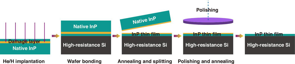
Figure 1: Fabrication of InPOS by ion-cutting.
The InPOS substrate process (Figure 1) began with a 2-inch InP source, which was exposed to a co-implant of helium and hydrogen (He/H) ions, creating a damaged layer of the crystal a short distance below the surface. This layer was bonded to 4-inch high-resistance silicon.
The InP and Si surfaces were activated before bonding by a fast atom beam (FAB) of argon (Ar) for 1 minute. The wafers were bonded in vacuum with a bonding pressure of 5MPa. The the applied InP was separated at the ion-damaged layer by 200°C annealing for 2 hours in nitrogen.
The remnants of the ion-damage at the InPOS surface were then removed using chemical mechanical polishing, leaving a smooth thin monocrystalline layer of InP on the silicon.
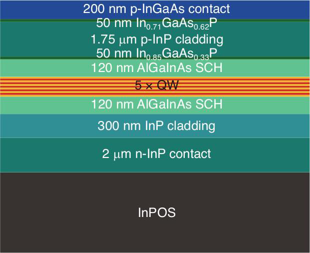
Figure 2: Laser epitaxial material structure.
The InPOS was used as substrate for metal-organic chemical vapor deposition (MOCVD) growth of aluminium gallium indium arsenide (AlGaInAs) heterostructures for 1.55μm-wavelength laser devices (Figure 2). The active multiple quantum well (QW) region consisted of 5 Al0.24Ga0.05In0.71As wells separated by Al0.44Ga0.07In0.49As barriers.
The growth process was optimized for MOCVD on bulk InP, not InPOS. Hence, standard material characterizations, such as x-ray diffraction and surface roughness, showed reduced material quality compared with structures grown on bulk InP.
The surface roughness of the heterostructure on InPOS was 0.4nm, compared with 0.2nm on bulk InP, according to atomic force microscopy (AFM). The team comments: “The InPOS surface after epitaxial growth with an RMS roughness value of 0.4nm is smooth enough to facilitate the device fabrication without any pinholes, which is essential for high-performance lasing.”
X-ray rocking curves from the InP (004) reflection showed a significant 2.88x increase in the peak width for the InPOS over bulk InP due to residual strain from the ion-cutting process. A small x-ray diffraction peak width indicates higher crystal quality. The MOCVD process only slightly altered the peak widths.
Photoluminescence measurements on the AlGaInAs structures (without cladding/contact layers) showed a 50% reduction in peak intensity for material on InPOS, compared with bulk InP. The full-width at half maximum (FWHM) values were 67.5meV and 70.0meV for materials on InPOS and bulk InP, respectively.
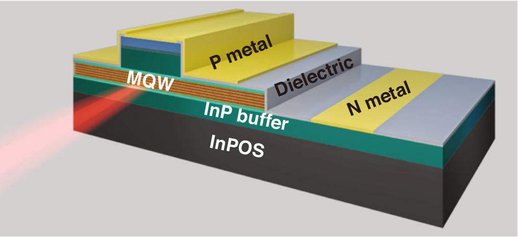
Figure 3: Ridge-waveguide laser scheme.
Ridge-waveguide Fabry-Pérot (FP) laser structures were fabricated from the materials (Figure 3).
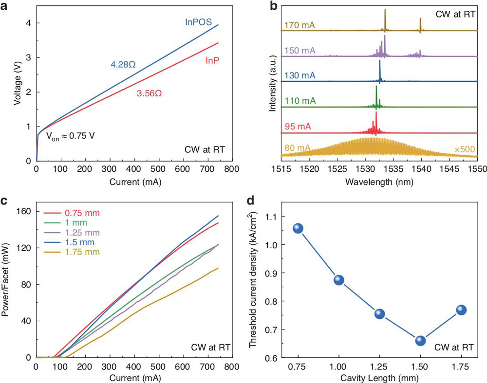
Figure 4: a Current-voltage behavior of as-cleaved lasers on bulk InP and InPOS with 8μmx1500μm ridge cavities. b Lasing spectra from InPOS laser. c Light output power versus current for laser on InPOS for various cavity lengths under CW operation. d Threshold current density (Jth) versus cavity length for lasers on InPOS.
The lasers were tested at 20°C, ‘room temperature’ (RT), under CW operation (Figure 4). The turn-on voltage (Von) was 0.75V for both the device types on bulk InP and InPOS substrates. Electrically, the InPOS devices had somewhat higher series resistance (4.28Ω). The higher resistance for the InPOS laser was attributed to the thinner InP layer (~2μm) through which the current had to travel from the N-electrode, reducing the cross-sectional area, compared with ~100μm for bulk InP.
The InPOS laser showed a decrease in Jth with increased cavity length up to 1500μm. An increase of Jth above that could be related to an improperly split facet in the 1750μm-long laser tested.
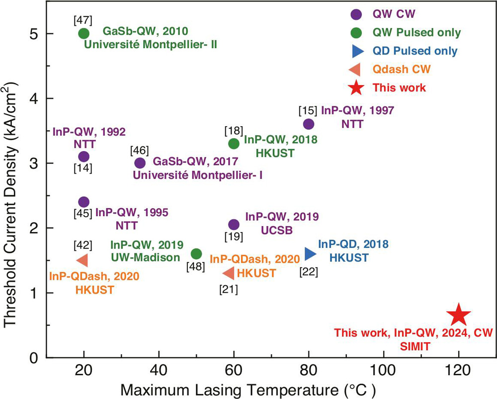
Figure 5: Historical evolution of 1.55μm-band lasers monolithically integrated on silicon by direct epitaxial growth in terms of threshold current density reduction and increase in maximum lasing temperature.
The researchers report (Figure 5): “The minimum Jth of 0.65kA/cm−2 was achieved with a cavity length of 1.5mm at RT under CW mode, which is the lowest Jth ever recorded for a silicon-based FP laser emitting at 1.55μm.”
The threshold is only slightly higher than the lowest value of 0.6kA/cm−2 demonstrated by silicon-based 1.55μm lasers integrated by other methods.
The single-facet output power for the InPOS laser reached 155mW at 740mA injection without saturation. The laser on bulk InP only reached a slightly higher value of 164mW. The team point out in particular that their InPOS laser emits much higher power than a 22mW CW result reported by the Hong Kong University of Science and Technology (HKUST) in 2020 for a 1.55μm-wavelength electrically pumped lasers grown directly by MOCVD on V-grooved silicon.
Raising operating temperatures typically degrades the performance of semiconductor lasers. The InPOS laser was found to continue operating up to 120°C, while that on bulk InP only reached 115°C.
The team comments: “It is impressive that the laser on the InPOS can operate at a higher temperature of 120°C. To the best of our knowledge, 120°C is the highest operating temperature achieved to date for the silicon-based FP laser emitting at 1.55μm under CW mode.”
Laser operation could be maintained for both InPOS and bulk InP devices at even higher temperature, up to the 130°C limit of the thermoelectric cooler (TEC), by adopting 2μs pulsed current injection to avoid self-heating (0.5% duty cycle).
The effect of self-heating was less prominent on InPOS lasers, compared with bulk InP, which the researchers attribute to the higher thermal conductivity of silicon (145W/m-K) compared with InP (68W/m-K). The threshold current reduction from adopting pulsed operation at 115°C was 20.7% for the InPOS laser, but for bulk InP it was 35.7%.
CW laser diodes on silicon InP SOI InPOS InPOS substrate MOCVD III-V epitaxy
https://doi.org/10.1038/s41377-024-01389-2
The author Mike Cooke is a freelance technology journalist who has worked in the semiconductor and advanced technology sectors since 1997.


