


News: LEDs
29 August 2024
Micro-LEDs on freestanding GaN
Researchers based in China have been exploring the benefits of using freestanding (FS) gallium nitride (GaN) as a substrate for micro light-emitting diodes (LEDs) [Guobin Wang et al, Optics Express, v32, p31463, 2024]. In particular, the team developed an optimized indium gallium nitride (InGaN) multiple quantum well (MQW) structure with improved performance at lower current injection (~10A/cm2) and lower driving voltages as suitable for the advanced micro-displays used in augmented (AR) and virtual reality (VR) setups where the higher cost of FS-GaN can be compensated by improved efficiency.
The researchers were associated with the University of Science and Technology of China, Suzhou Institute of Nano-Tech and Nano-Bionics, Jiangsu Institute of Advanced Semiconductors, Nanjing University, Soochow University, and Suzhou Nanowin Science and Technology Co Ltd. The team sees opportunities for such micro-LEDs in displays with ultra-high pixels per inch (PPI) sub-micro or nano-LED configurations.
The researchers compared the performance of micro-LEDs fabricated on freestanding GaN and GaN/sapphire templates (Figure 1).
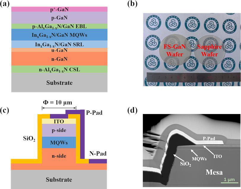
Figure 1: a) Micro-LED epitaxial scheme, b) micro-LED epitaxial wafers, c) micro-LED chip structure, and d) cross-sectional transmission electron microscope (TEM) image.
The metal-organic chemical vapor deposition (MOCVD) epitaxial structure included a 100nm n-type aluminium gallium nitride (n-AlGaN) carrier diffusion/spreading layer (CSL), a 2μm n-GaN contact layer, a 100nm low-silane unintentionally-doped (u-)GaN high-electron-mobility layer, a 20x(2.5nm/2.5nm) In0.05Ga0.95/GaN strain-release layer (SRL), 6x(2.5nm/10nm) blue InGaN/GaN MQW, a 8x(1.5nm/1.5nm) p-AlGaN/GaN electron-blocking layer (EBL), an 80nm p-GaN hole injector, and a 2nm heavily doped p+-GaN contact layer.
The materials were fabricated into 10μm-diameter LEDs with indium tin oxide (ITO) transparent contact and silicon dioxide (SiO2) sidewall passivation.
Chips from the heteroepitaxy GaN/sapphire template showed much wider variations in performance. In particular, the intensity and peak wavelengths varied much more according to position within the chip. One chip on sapphire showed a 6.8nm wavelength shift between the center and edge at 10A/cm2 current density. Two chips sourced from the sapphire wafer had one with only 76% intensity compared with the other.
For chips fabricated on FS-GaN the wavelength variation was reduced to 2.6nm, and two different chips showed much more comparable intensity performance. The researchers attribute the wavelength uniformity variation to the different stress states in the homo- and hetero-structures: the residual stresses were 0.023GPa and 0.535GPa, respectively, according to Raman spectroscopy.
Cathodoluminescence showed dislocation densities of ~108/cm2 for heteroepitaxial wafers and ∼105/cm2 for homoepitaxial wafers. “Lower dislocation density can minimize the leakage pathways and enhance luminous efficiency,” the team comments.
Although the reverse leakage current was reduced for the homoepitaxy LEDs, the current response under forward bias was also reduced, relative to the heteroepitaxy chips. Despite the lower current, the chips on FS-GaN showed higher external quantum efficiency (EQE): in one case, 14%, compared with 10% on the sapphire template. By comparing photoluminescence performances at 10K and 300K (room temperature), the internal quantum efficiencies (IQEs) were estimated to be 73.2% and 60.8%, respectively.
Based on simulation work, the researchers designed and realized an optimized epitaxial structure on FS-GaN that improved EQE and voltage performance at the lower current injections of micro-displays (Figure 2). In particular, the homoepitaxy enables thinner barriers with sharp interfaces, while the same structure implemented in heteroepitaxy shows more blurred outlines under TEM examination.
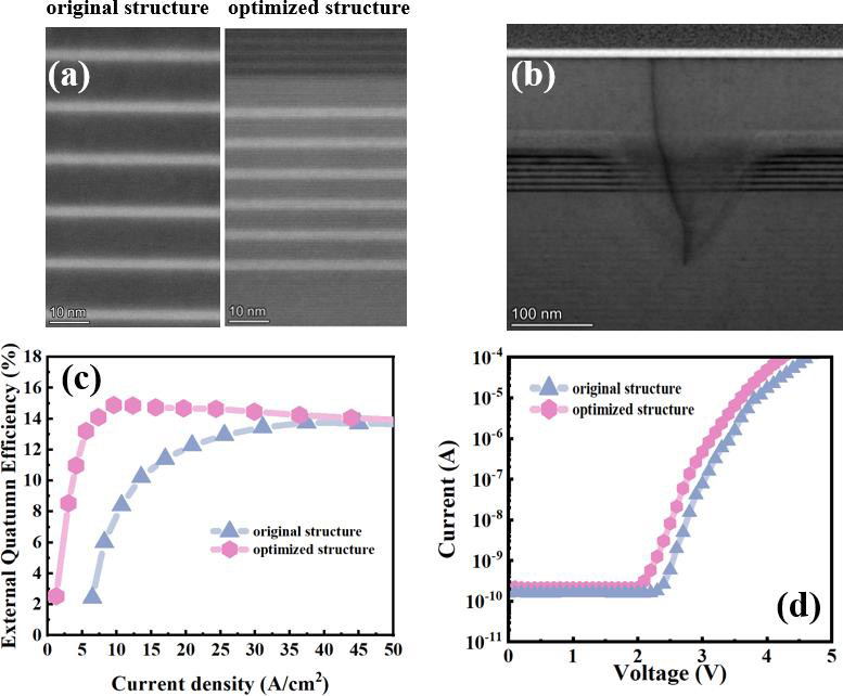
Figure 2: TEM images of MQW regions for a) original and optimized homoepitaxial structures, b) optimized structure implemented in heteroepitaxy, c) EQE and d) current-voltage curves of homoepitaxial micro-LED chips.
The thinner barriers to some extent emulates what happens with V-pits that tend to form around dislocations. V-pits have been found to have beneficial performance effects in heteroepitaxial LEDs, such as improved hole injection into the light-emitting region, partly due to barrier thinning in MQW structures around the V-pit.
The homoepitaxial LEDs showed an EQE increase from 7.9% to 14.8% at 10A/cm2 injection. The voltage needed for driving 10μA current was reduced from 2.78V to 2.55V.
Micro-LEDs Freestanding GaN GaN MOCVD
https://doi.org/10.1364/OE.529771
The author Mike Cooke is a freelance technology journalist who has worked in the semiconductor and advanced technology sectors since 1997.


