


News: LEDs
1 August 2024
Strain-engineering for green LEDs on silicon
Researchers report on improved 78% internal quantum efficiency (IQE) for green indium gallium nitride (InGaN) light-emitting diode (LED) epitaxial structures grown on silicon (Si) using only a single aluminium nitride (AlGaN) buffer layer [Yayu Dai et al, Appl. Phys. Lett., v125, p022102, 2024]. Although electroluminescence results were not presented, the IQE boost could lead to more power-efficient standard and micro-LEDs for green and red wavelengths.
For blue LEDs produced on silicon it is typical to use both an AlN nucleation layer and step-graded AlGaN buffer to bridge the large thermal expansion mismatch between silicon and GaN. GaN templates grown on such a buffer structure tend to have a residual compressive stress when the temperature is cooled to room temperature, which inhibits indium incorporation in the subsequent InGaN layers that are used to emit visible light. For longer green and red emissions, even more indium is needed in the InGaN layers than for blue.
The proper strain management of GaN-on-Si is of paramount importance to fabricate the InGaN-based long-wavelength micro-LEDs grown on silicon toward full-color micro-displays,” explains the team drawn from University of Science and Technology of China, Suzhou Institute of Nano-Tech and Nano-Bionics, Guangdong Institute of Semiconductor Micro-nano Manufacturing Technology, and Suzhou LEKIN Optoelectronics Technology Co Ltd.
There are substrates other than silicon that can be used to produce LEDs, but these are smaller, and usually much more expensive. Not only does silicon come in large diameters, enabling low-cost mass production, but also most drive systems are based on silicon electronics. Monolithic integration of the drive and light-emission components could further reduce electronic system complexity and cost.
The epitaxial materials (Figure 1) were grown by metal-organic chemical vapor deposition (MOCVD) on silicon. Two samples were processed, one using a conventional step-graded AlGaN buffer on AlN, the other using just an AlN buffer before the n-GaN contact/buffer/template layer.
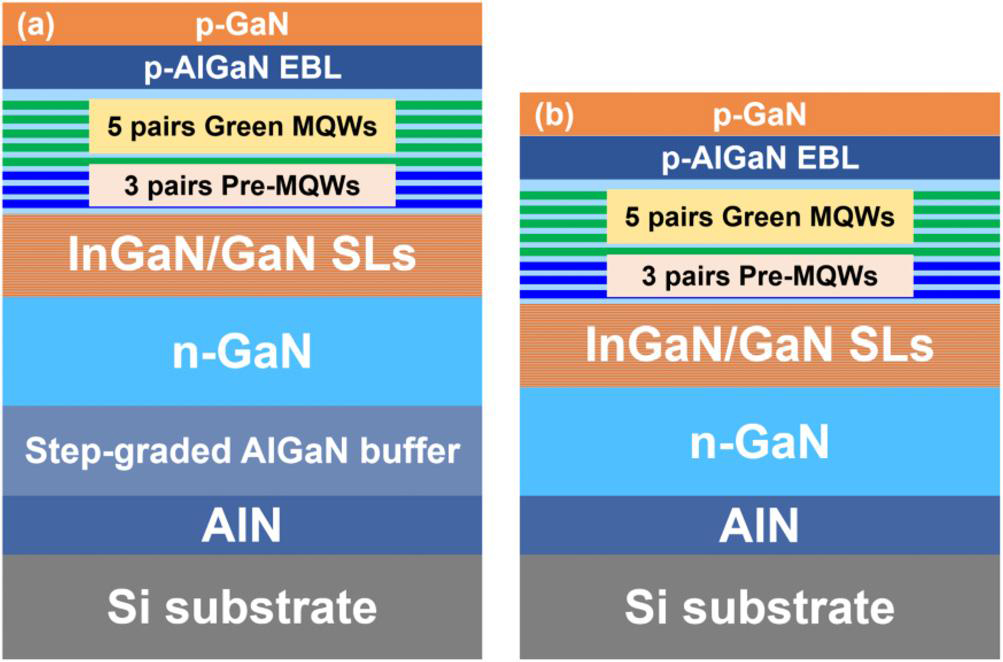
Figure 1: InGaN-based green LED schemes: (a) Sample A with Al-composition step-graded AlN/AlGaN multiple-layer buffer and (b) sample B with AlN single-layer buffer.
The researchers report of the conventional sample A: “The Al-composition step-graded AlN/AlGaN multiple-layer buffer used in GaN template A in this work is commercially available and has been used in the mass production of GaN-on-Si blue LEDs, showing high efficiency and great reliability.”
X-ray analysis gave a higher threading dislocation (TD) density for the sample B 2μm GaN template than for sample A: 2.5x10⁹/cm2 and 9.0x10⁸/cm2, respectively. The further green InGaN LED layers were grown by co-loading both samples into a MOCVD chamber.
The LED structure consisted of 160nm In0.05Ga0.95N/GaN superlattice (SL), multiple quantum wells (MQWs), a 20nm electron-blocking layer and a 35nm p-GaN contact layer. The MQW light-emitting region consisted of three pre-wells of 2nm blue-emitting In0.12Ga0.88N/GaN, and five wells of 2.5nm green-emitting In0.25Ga0.75N/GaN. The wells were separated by 10nm GaN barriers.
Micro-photoluminescence (PL) analysis (Figure 2) showed sample B to have a more homogeneous emission pattern than sample A. Further, B’s pattern had no visible dark spots, unlike sample A. The researchers comment: “The dark spots in micro-PL images typically represent non-radiative recombination centers caused by thermal degradation of the InGaN MQWs.”
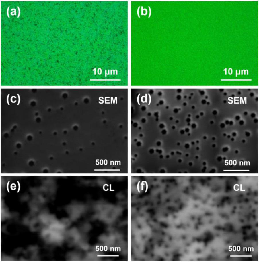
Figure 2: Micro-PL, top-view SEM and panchromatic CL images of InGaN MQWs for sample A (a), (c) and (e) and sample B (b), (d) and (f), respectively.
Further inspections using a scanning electron microscope (SEM) and cathodoluminescence (CL) showed V-pit densities for sample A and B of 7.0x10⁸/cm2 and 2.0x10⁹/cm2, respectively. These values are consistent with the threading dislocation values. V-pits generally form on threading dislocations.
The team comments: “It has been theoretically and experimentally confirmed that V-pits with thinner QWs at the sidewalls can generate a potential barrier and screen the effect of TDs, which facilitates hole injection and enhances radiative recombination, regarded as an effective method to improve the efficiency of InGaN-based LEDs.”
So, a higher threading dislocation density is not necessarily a bad thing. The CL images showed A to have dark spot clusters, which show up as dark spots at the optical microscope level, while sample B’s CL spots are more evenly spread, giving a better optical morphology.
The PL spectra showed sample B to have longer 40nm red-shifted peak relative to sample A. Raman spectroscopy also showed that sample B was almost strain-free, unlike sample A. The compressive stress in sample A was estimated to be 0.37GPa (sample B’s stress was ~0GPa).
The researchers comment: “The Raman spectra confirm that the AlN single-layer buffer used in the GaN template B can effectively relax the residual compressive stress of the subsequent GaN layer, which is expected to reduce the misfit strain between GaN and InGaN, thus facilitating the indium incorporation of InGaN MQWs.”
High-angle annular dark field (HAADF) scanning transmission electron microscopy (STEM) images also showed degradation of the MQW structure in sample A relative to B due to the residual strain (Figure 3).
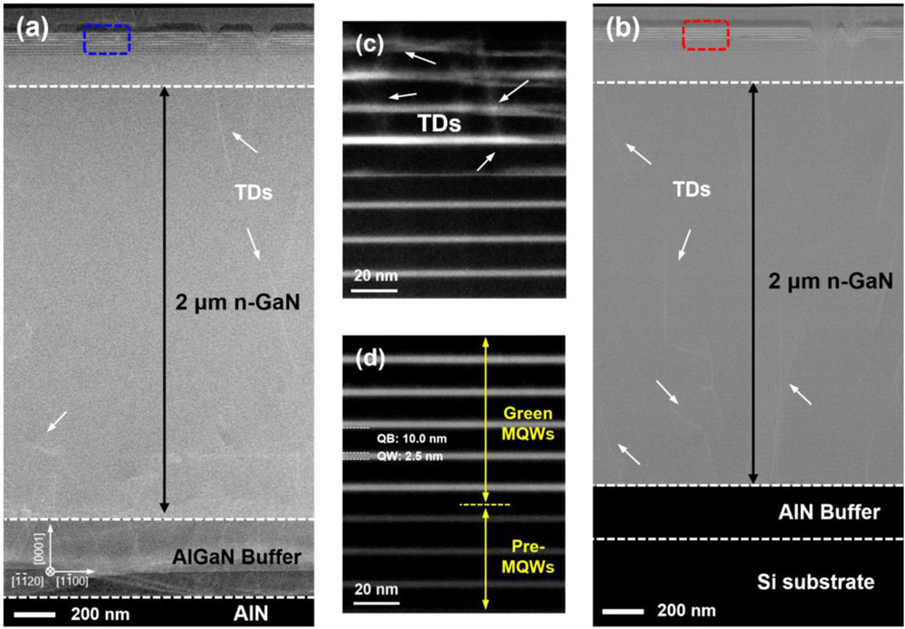
Figure 3: Cross-section HAADF-STEM images of InGaN-based LED material for (a) sample A and (b) sample B, and enlarged images of active MQW regions marked with blue and red rectangles for (c) sample A and (d) sample B.
By comparing the PL intensity at 5K and 300K, the researchers estimate the room-temperature internal quantum efficiency (IQE) at 33% and 78% for samples A and B, respectively.
The researchers also performed a time-resolved PL study, extracting fast (τ1) and slow (τ2) lifetimes. The researchers comment on τ1 that it reflects carrier transfer from weakly to strongly localized states. The slow τ2 decay is related to carrier recombination in the localized states.
Table 1: IQE, τ1,τ2, τ2r and τ2nr of samples A and B.
Sample |
IQE |
τ1 |
τ2 |
τ2r |
τ2nr |
| A | 33% | 2.9ns | 24.6ns | 74.5ns | 36.7ns |
| B | 78% | 1.8ns | 38.4ns | 49.2ns | 174.5ns |
The researchers combined the slow decay rates with their knowledge of the slow decays to present radiative (τ2r) and non-radiative (τ2nr) lifetimes (Table b).
Green LEDs AlN InGaN Si substrate GaN MOCVD
https://doi.org/10.1063/5.0218897
The author Mike Cooke is a freelance technology journalist who has worked in the semiconductor and advanced technology sectors since 1997.


